Capacitor and manufacturing method
A manufacturing method and capacitor technology, which are applied in the directions of multilayer capacitors, fixed capacitor electrodes, fixed capacitor dielectrics, etc., to achieve the effect of reducing stress concentration
Inactive Publication Date: 2003-12-31
PANASONIC CORP
View PDF1 Cites 8 Cited by
- Summary
- Abstract
- Description
- Claims
- Application Information
AI Technical Summary
Problems solved by technology
In addition, especially when the upper electrodes 116, 116A, 116B and the lower electrodes 112 are formed by vapor
Method used
View moreImage
Smart ImageViewing Examples

Examples
 PUM
| Property | Measurement | Unit |
|---|---|---|
| Thickness | aaaaa | aaaaa |
| Thickness | aaaaa | aaaaa |
| Slope | aaaaa | aaaaa |
Abstract
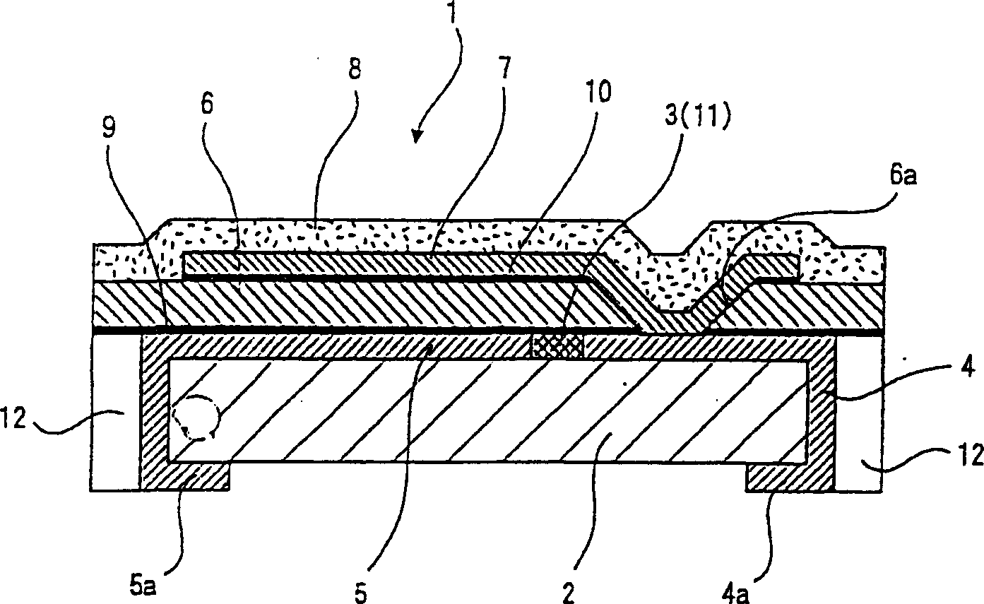
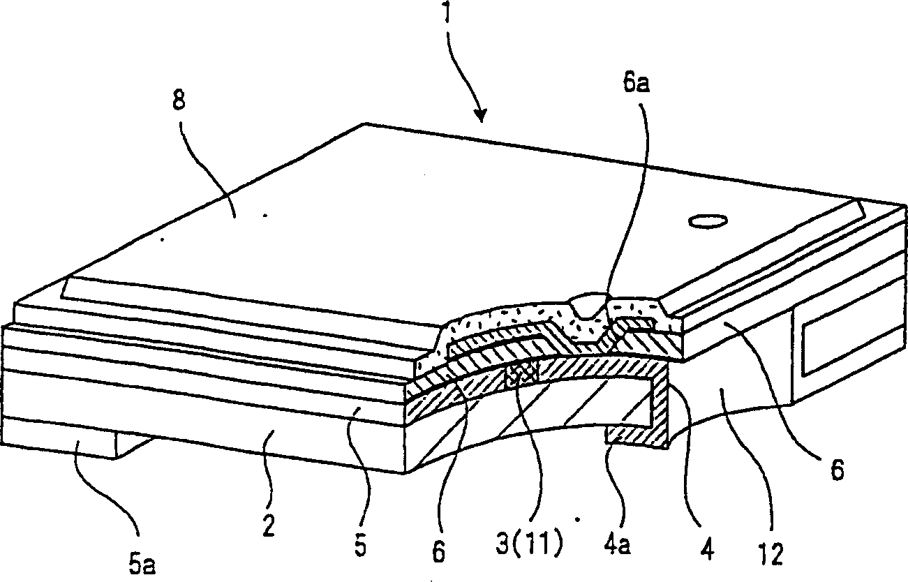
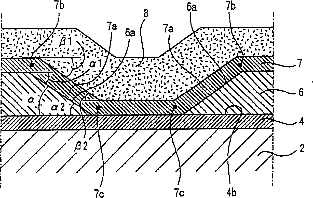
A capacitor (1) using a flexible substrate (2) includes a hole portion (6a) formed in a dielectric (6) to connect an upper electrode (7) to an external leader electrode (4). At least part of the hole portion ( 6a) extends from its lower end to upper end at an inclination between 0.1 and 20 DEG with respect to a top surface of the external leader electrode (4). Then, an upper end corner of an inclined wall surface of the upper electrode (7), which inclines along the hole portion (6a) of the dielectric (6), has a downward inclination between 0.1 and 20 DEG . A lower end corner of the inclined wall surface of the upper electrode (7), which inclines along the hole portion of the dielectric (6), has an upward inclination between 0.1 and 20 DEG . As a result, stress concentration on the corners of the upper electrode (7) is drastically reduced to prevent the upper electrode (7) from cracking.
Description
technical field [0001] The present invention relates to capacitors and methods for their manufacture. Background technique [0002] As a conventional small capacitor, it is known that an electrode portion composed of a thin-film dielectric layer and a metal film is formed on a relatively rigid substrate such as ceramics or epoxy resin. However, for such a capacitor, although the thin film dielectric layer or the electrode part can be made very thin, if the substrate does not have a certain thickness (for example, 0.5mm), there is a risk of cracking and damage. Thinness has a certain limit, and it is difficult to use such capacitors for products that are not even 1mm thick. [0003] As a capacitor that meets this requirement, for example, disclosed in Japanese Patent Laid-Open No. 11-97287, there is a film-shaped flexible capacitor composed of a highly flexible organic resin substrate such as polyimide with a thickness of less than 0.1 mm. substrate capacitors. According t...
Claims
Login to View More Application Information
Patent Timeline
 IPC IPC(8): H01G4/005H01G4/06H01G4/33
CPCH01G4/33C22C38/14H01G4/005C22C38/002B22F9/007H01F1/0574C22C38/005C22C38/12B22F9/008H01G4/06B22F2999/00H01F1/0579H01F1/058B82Y25/00C22C1/0441
Inventor 渡边久芳今中崇内田徹仙石修糸井真介西原宗和東田隆亮末次大輔山本憲一勝部淳久村博隆
Owner PANASONIC CORP
Features
- Generate Ideas
- Intellectual Property
- Life Sciences
- Materials
- Tech Scout
- Unparalleled Data Quality
- Higher Quality Content
- 60% Fewer Hallucinations
Learn More Browse by: Latest US Patents, China's latest patents, Technical Efficacy Thesaurus, Application Domain, Technology Topic, Popular Technical Reports.
© 2025 PatSnap. All rights reserved.Legal|Privacy policy|Modern Slavery Act Transparency Statement|Sitemap|About US| Contact US: help@patsnap.com