

Passivation encapsulation method for organic electro luminescence elements and structure
A packaging structure and packaging method technology, applied to electrical components, lighting devices, light sources, etc., can solve the problems of high cost, high equipment cost, poor barrier layer coverage, high production cost, etc., to improve the step effect, simplify the manufacturing process, improve The effect of production efficiency
- Summary
- Abstract
- Description
- Claims
- Application Information
AI Technical Summary
Problems solved by technology
Method used
Image

Examples
Embodiment Construction
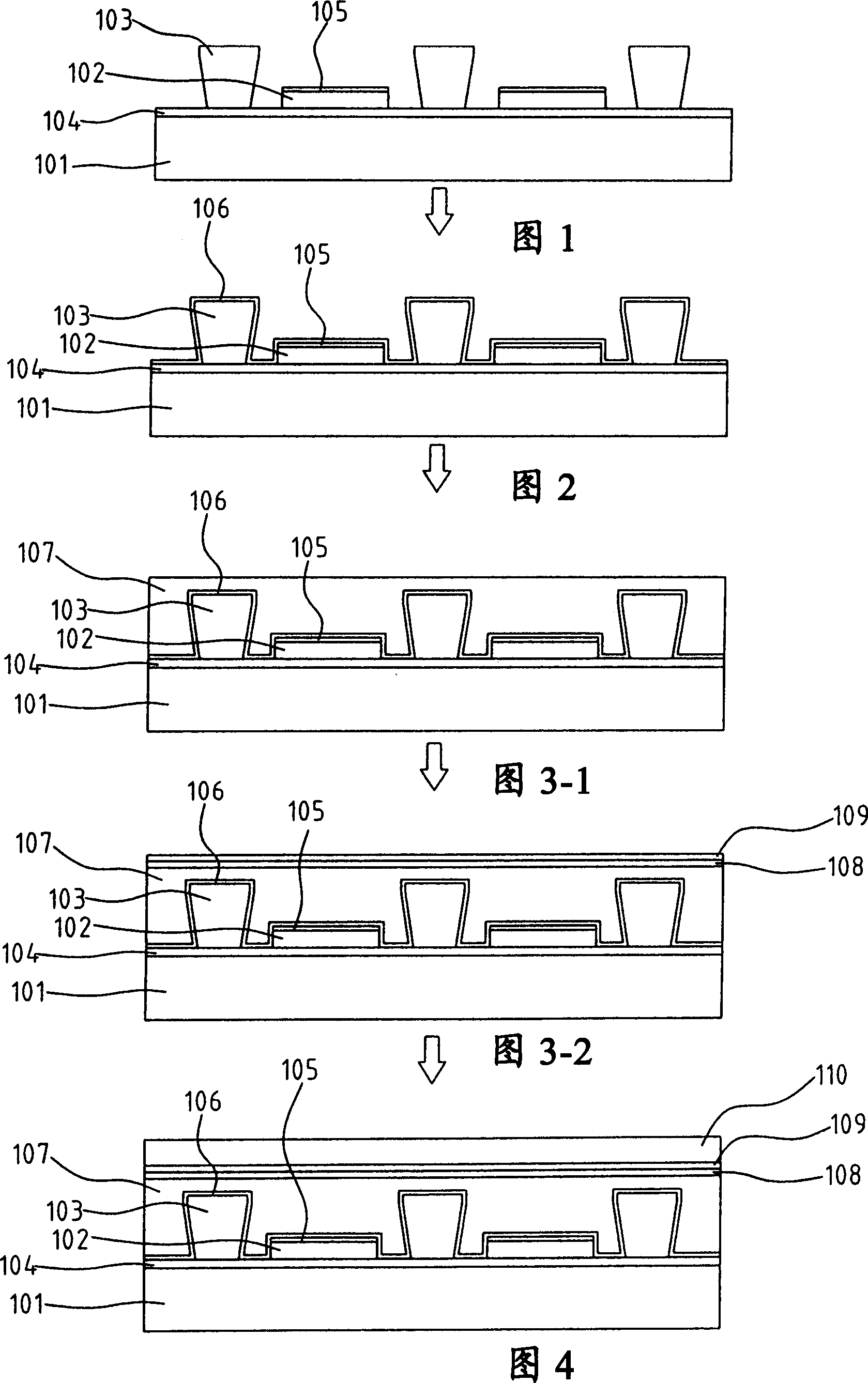
[0026] As shown in Fig. 1~Fig. 4, be embodiment of the present invention, show a kind of barrier (passivation) encapsulation method of organic EL element, this method comprises the following steps:
[0027] As shown in Figure 1, for the step of providing a transparent substrate 101, a plurality of organic EL element pixels 102 have been formed on the transparent substrate 101, and have a plurality of ribs (rib) 103; There is an ITO anode layer 104 as the anode of the organic EL element pixel 102, and the organic EL element pixel 102 has a cathode layer 105 on the upper surface, and the purpose of designing the ribs 103 is to prevent the cross talk phenomenon of the element.
[0028] As shown in Figure 2, for the step of forming a protective layer, a cathodic protective layer 106 is plated on the surface of the organic EL element pixel 102, which is an inorganic material layer; and the protective layer 106 is formed by a low-temperature chemical vapor deposition method Formed b...
PUM
 Abstract
Description
Claims
Application Information