Bias voltage forming circuit, amplifying circuit, streamline type AD adaptor

一种偏压电压、偏压电路的技术,应用在模数转换器、直流耦合的直流放大器、改进放大器以提高效率等方向,能够解决电路面积增大、消耗超过功率等问题

Inactive Publication Date: 2004-09-29
SANYO ELECTRIC CO LTD
View PDF2 Cites 6 Cited by
  • Summary
  • Abstract
  • Description
  • Claims
  • Application Information

AI Technical Summary

Problems solved by technology

[0006] In the above-mentioned amplifying circuit, since the bias voltage is always applied regardless of the content of the operation, it consumes more than necessary power
On the other hand, even if power saving is achieved by turning off the bias voltage for a long time during the standby period that does not require power, components such as capacitors must be provided to reduce the leakage during the off period, and there is a problem that the circuit area increases.

Method used


Image

  • Bias voltage forming circuit, amplifying circuit, streamline type AD adaptor
  • Bias voltage forming circuit, amplifying circuit, streamline type AD adaptor
  • Bias voltage forming circuit, amplifying circuit, streamline type AD adaptor

Examples


no. 1 Embodiment approach

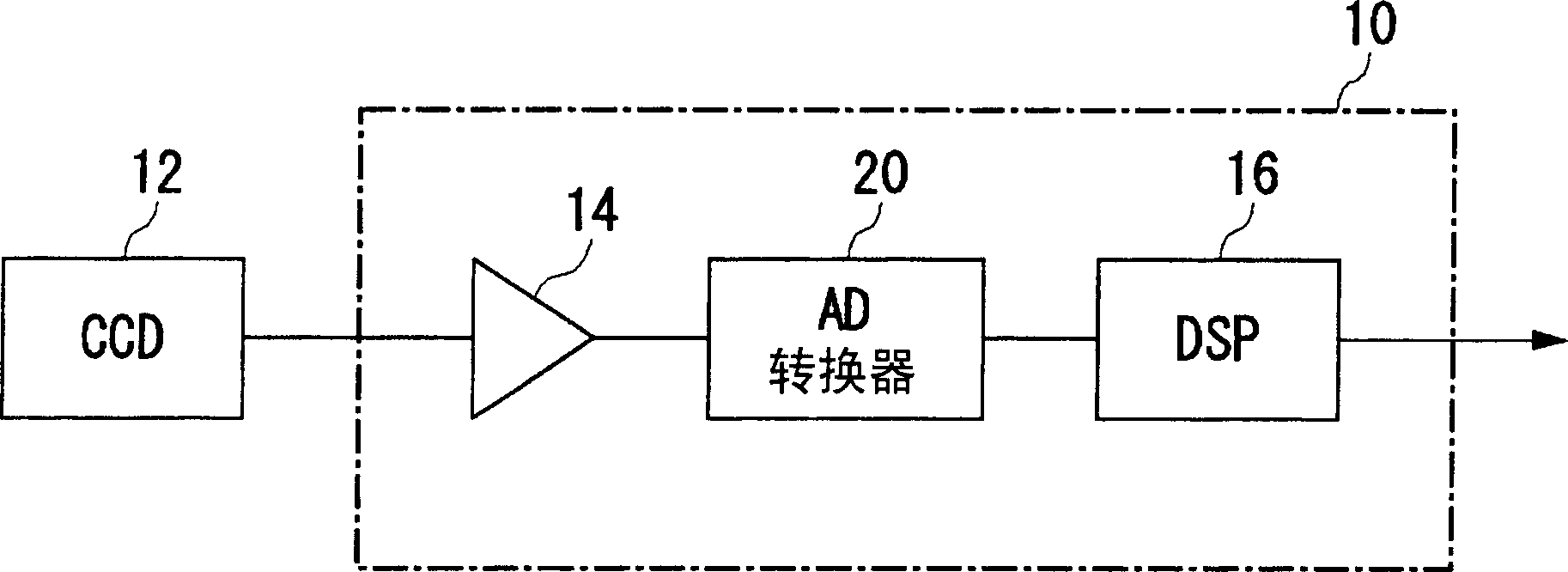
[0026] figure 1 It shows the basic configuration of an image processing circuit partially including the bias voltage generating circuit of this embodiment. An image sensor 12 such as a CDD (Charge Coupled Device) or a CMOS sensor takes in light from a subject, converts it into an electrical signal, and inputs it to a single-chip LSI (Large Scale Integration) 10 . In the single-chip LSI 10 , an AGC (Auto Gain Control) 14 , an AD converter 20 , and a DSP (Digital Signal Processor) 16 are incorporated. The AGC 14 amplifies the electrical signal received from the image sensor 12, the AD converter 20 converts the amplified analog signal into a digital signal, and the DSP 16 performs processing such as compression on the converted digital signal. Each structure built in the monolithic LSI 10 is powered by a predetermined voltage power supply.

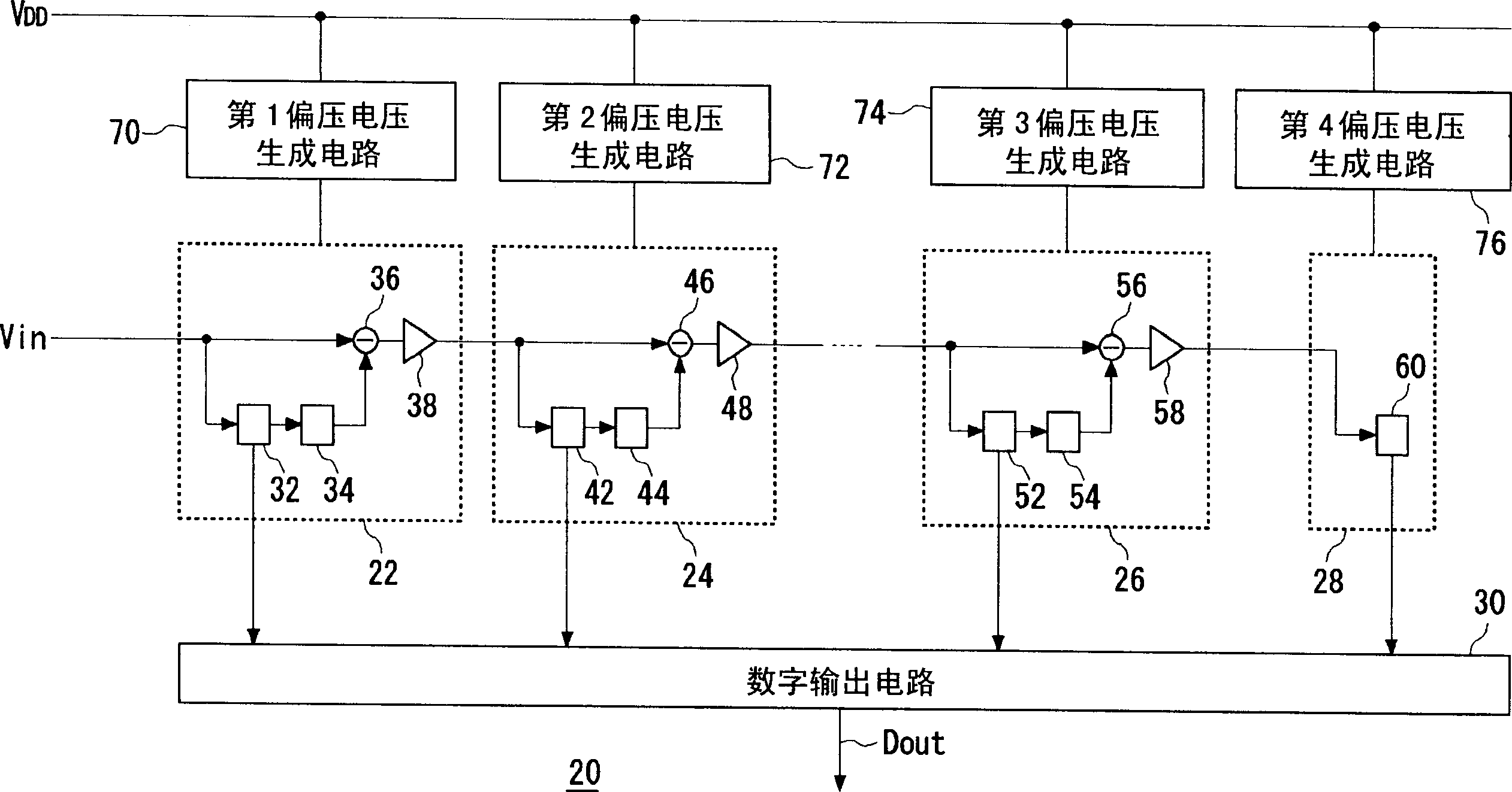
[0027] The AD converter 20 includes a bias voltage generating circuit for realizing low power consumption, and realizes low power consumpt...

no. 2 Embodiment approach

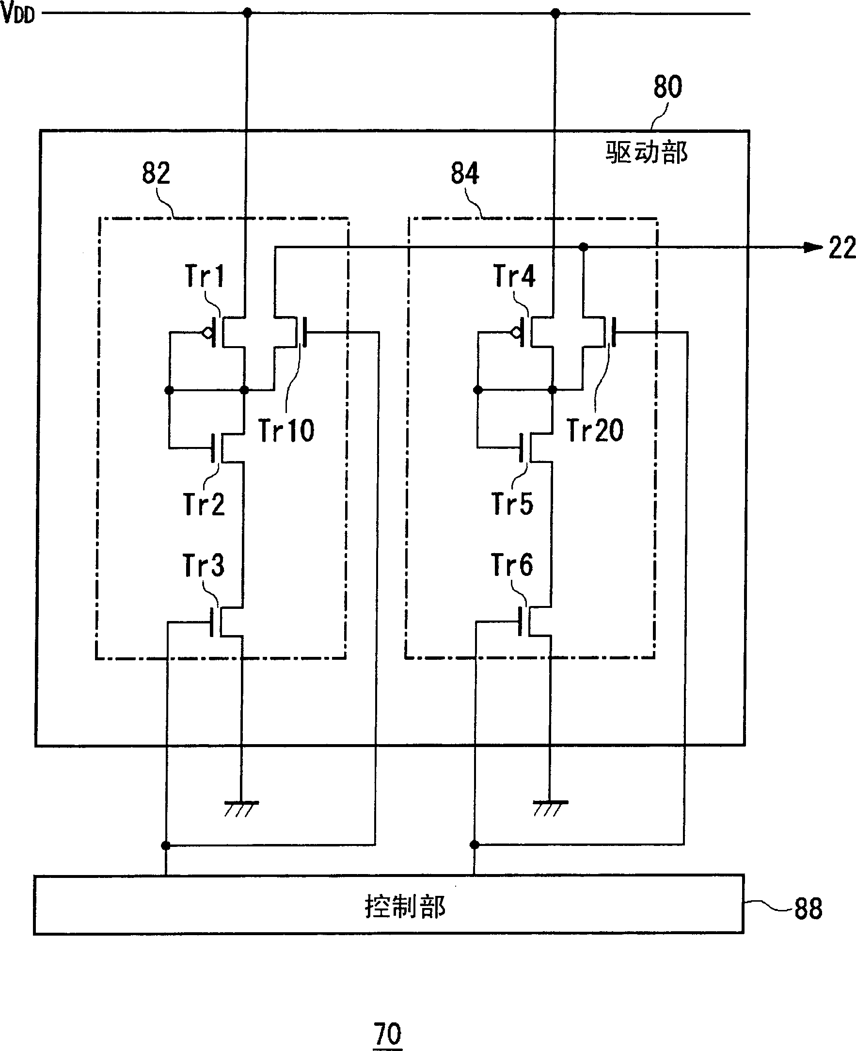
[0043] The difference between the bias voltage generation circuit of this embodiment and the first embodiment lies in the control timing of the first bias circuit and the second bias circuit of the control unit, but the other configurations are the same as those of the first embodiment.

[0044] The implementation is the same.

[0045] Figure 5 It is a timing chart showing the relationship between the change in the operation of the first conversion unit 22 and the control of the control unit 88 in the second embodiment. In the present embodiment, during the auto-zero operation period, especially immediately after the auto-zero start, a large current is required, and a small current is sufficient for the remaining auto-zero period. Correspondingly, the control unit 88 turns on both the third transistor Tr3 and the sixth transistor Tr6 during the period immediately after the auto-zero start, turns off the third transistor Tr3 during the remaining auto-zero period, and turns on...

no. 3 Embodiment approach

[0047] The bias voltage generating circuit of the present embodiment differs from the first and second embodiments in that the current driving capabilities of the plurality of bias circuits constituting the drive unit are all the same, but the other configurations are the same as those of the first or second embodiments. same.

[0048] Figure 6 The configuration of the first bias voltage generating circuit 70 is shown. In the first bias generation circuit 70 , the drive unit 80 includes a first bias circuit 82 , a second bias circuit 84 , and a third bias circuit 86 . These bias circuits have the same current drive capability. That is, the element sizes and size ratios of the first and second transistors Tr1 and Tr2 constituting the first bias circuit 82, the element sizes and size ratios of the fourth and fifth transistors Tr4 and Tr5 constituting the second bias circuit 84, and the configuration The element sizes and size ratios of the seventh and eighth transistors Tr7 ...


PUM


Abstract

A first bias voltage generating circuit which applies a bias voltage to an amplifier circuit of an AD converter has a driving unit and a control unit. The driving unit includes a first bias circuit and a second bias circuit as a plurality of bias circuits which are connected in parallel and have different current driving capabilities. The first bias circuit and the second bias circuit each include a CMOS transistor which is connected directly between a power supply potential and a ground potential, and a switching element which interrupts a feedthrough current. The drains of the CMOS transistors output the bias voltage. The control unit turns on both or either one of the first bias circuit and the second bias circuit, thereby controlling the current driving capability of the entire driving unit.

Description

technical field [0001] The invention relates to a bias voltage generating circuit and an amplifying circuit. In particular, the present invention relates to techniques for controlling bias circuits. Background technique [0002] In recent years, mobile phones have been equipped with various additional functions such as image capture function, image playback function, video capture function, and video playback function, and there is a strong demand for reduction of power consumption of built-in amplifier circuits. In particular, single-chip LSIs incorporating analog-to-digital converters (hereinafter referred to as AD converters) have been miniaturized year by year, requiring a further reduction in power supply voltage. As an AD conversion circuit with high conversion accuracy, a multi-stage pipeline AD converter is known (for example, refer to Patent Document 1). Also, a technique is known in which an operational amplifier is incorporated in an AD converter, and an output ...

Claims


Application Information

Patent Timeline
Patent Type & Authority Applications(China)
IPC IPC(8): H03F3/34G11C5/14H03F3/42
CPCG11C5/145
Inventor 谷邦之和田淳
Owner SANYO ELECTRIC CO LTD
Why Eureka
Try Eureka