

Conductive pattern check-up apparatus
A conductive pattern and inspection device technology, which is applied in measurement devices, electrical measurement, and electrical variable measurement, etc., can solve the problems of being easily affected by noise, unreliable inspection, and small voltage value of conductive patterns, and achieves the effect of simple inspection.
- Summary
- Abstract
- Description
- Claims
- Application Information
AI Technical Summary
Problems solved by technology
Method used
Image

Examples
Embodiment 2
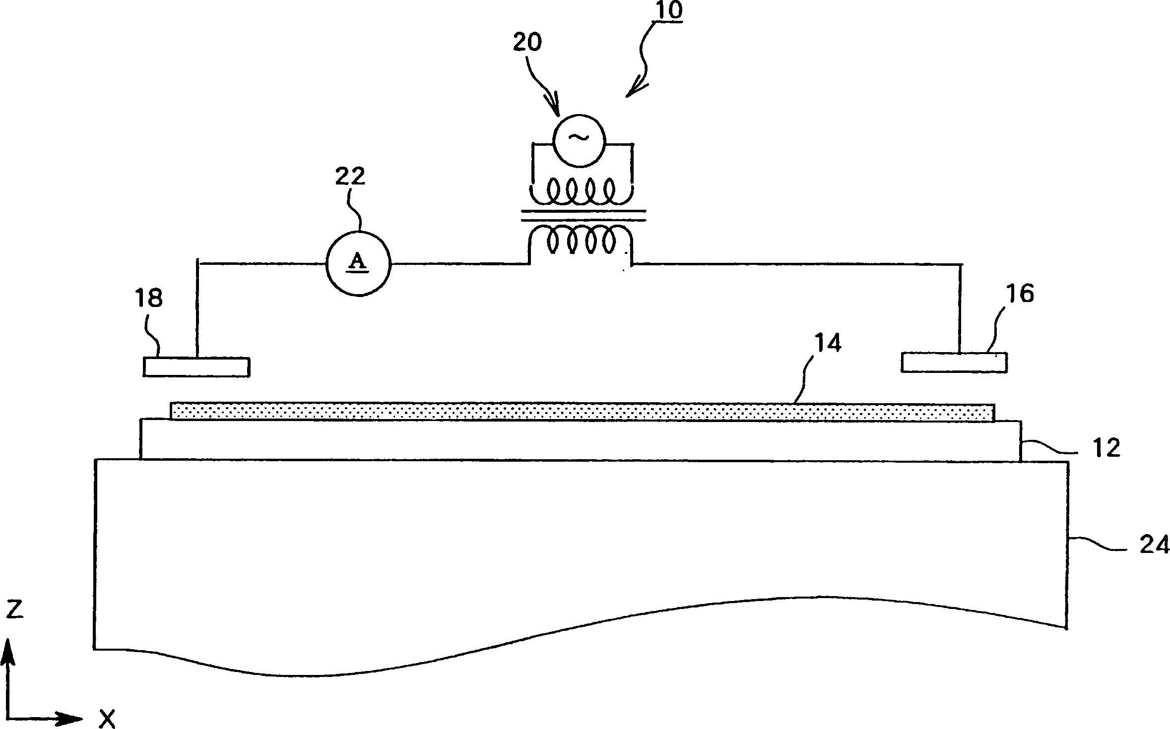
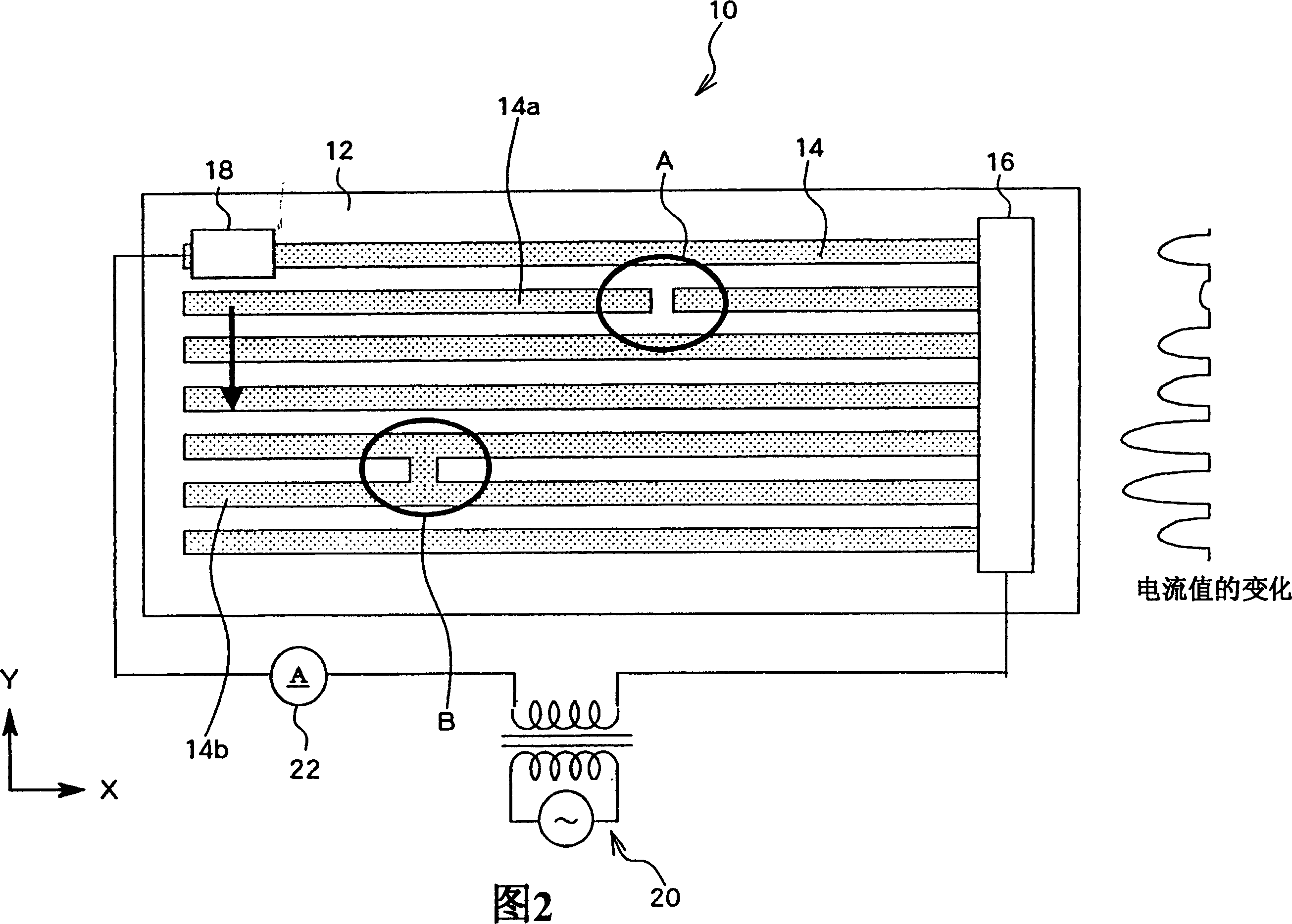
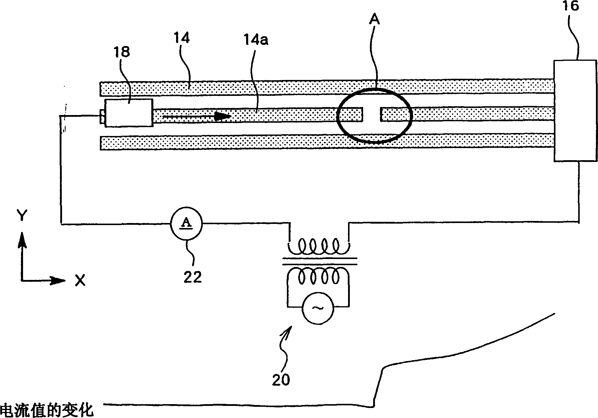
[0050] Next, a case where a common bar is used as a feeding electrode will be described.
[0051] Usually, in the conductive pattern 14 , in order to prevent damage to the conductive pattern due to static electricity, one end of all the conductive patterns is connected by a conductive sheet called a common bar. In the case of such a glass substrate, the common bar can also be used as a feeding electrode.
[0052] Specifically, as shown in FIG. 5 , an AC signal is applied to the conductive pattern 14 via the sensor electrode 18 and the common strip 30 . In this case, for feeding power to the common bar 30 , for example, a single-contact contact probe or the like may be used. Since the common bar 30 is physically and electrically connected to one end of all the patterns, it has the same function as the above-mentioned feeding electrode.
[0053] Therefore, when the sensor electrode 18 is moved in the Y direction, the current value detected by the current detector 22 is as show...
Embodiment 3
[0056] Next, other embodiments will be described.
[0057] Image 6 It is a schematic plan view of a pattern inspection device 10 as another example. In this pattern inspection device 10, a pair of first electrodes 32 provided at both ends of the pattern and a pair of second electrodes 34 provided on both sides of the pattern to be inspected are used as feeding electrodes. In addition, defect inspection is performed based on the voltage value of the sensor electrode 36 provided on the inspection target pattern.
[0058] The pair of first electrodes 32 are conductive sheets positioned above both ends of the conductive pattern 14 during inspection, and function as feeding electrodes for disconnection inspection. The first electrode 32 has a width covering the ends of all the patterns, and is electrostatically coupled to the ends of all the conductive patterns 14 . However, as long as the first electrode 32 has a width covering three or more pattern ends including the inspecti...
Embodiment 4
[0082] Next, a pattern inspection device 10 as another example will be described.
[0083] This pattern inspection device 10 is used especially for inspection of gate patterns and Cs patterns arranged on glass substrates used in liquid crystal display panels.
[0084] In the manufacturing process of the liquid crystal display panel, firstly, the gate pattern and the Cs pattern are arranged on the glass substrate 12 at the same time. The gate pattern is a plurality of conductive patterns arranged in columns on the glass substrate. The Cs pattern is a conductive pattern alternately arranged in a column. Since the distance between the gate pattern and the Cs pattern is extremely small (for example, several tens of um), a short circuit is easily generated. The pattern inspection apparatus 10 especially suitable for this short-circuit inspection is demonstrated.
[0085] FIG. 9 shows a schematic plan view of the pattern inspection device 10 .
[0086] The gate pattern 50 and th...
PUM
 Abstract
Description
Claims
Application Information