Semiconductor memory device
一种存储装置、半导体的技术,应用在信息存储、静态存储器、数字存储器信息等方向,能够解决数量增加、存储器面积增大等问题,达到削减电力消耗的效果
- Summary
- Abstract
- Description
- Claims
- Application Information
AI Technical Summary
Problems solved by technology
Method used
Image

Examples
no. 1 Embodiment approach
[0038] figure 1 The configuration of the semiconductor memory device according to the first embodiment of the present invention is shown.
[0039] In the same figure, a plurality of memory cells 100 (only 2 are shown in the same figure) are arranged in an array, and each memory cell 100, such as Figure 7 As shown, it is composed of 6 transistors including two load transistors MP1 and MP2, two drive transistors MN1 and MN2, and two conversion transistors MN3 and MN4. The sources of the two load transistors MP1 and MP2 are connected to a given power supply VDD, and the drains are connected to the sources of the conversion transistors MN3 and MN4 and the drains of the drive transistors MN1 and MN2. In addition, the gates of the two load transistors MP1 and MP2 are respectively connected to the gates of the drive transistors MN1 and MN2 and the drains of the other load transistors MP2 and MP1 . Furthermore, the sources of the two driving transistors MN1 and MN2 are connected t...
no. 2 approach
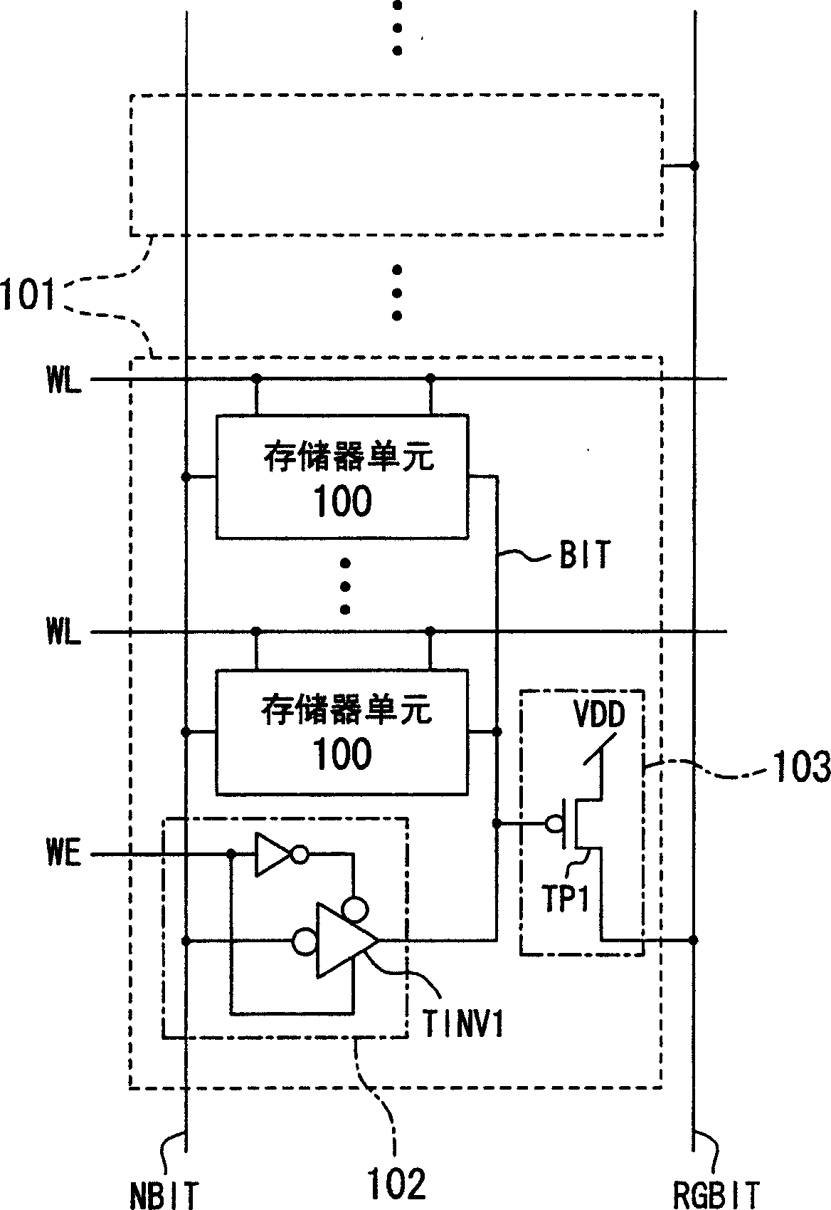
[0051] figure 2 The configuration of the semiconductor memory device according to the second embodiment of the present invention is shown.
[0052] exist figure 2 In the above-mentioned first embodiment, a plurality of memory cells 100 are arranged in an array, and at least two or more memory cells 100 are connected to the same bit line pair BIT, NBIT to form one memory cell group 101 .
[0053] For a plurality of memory cell groups 101 arranged in the bit line direction, one bit line NBIT is commonly connected, and at the same time, the other bit line BIT in each memory cell group 101 is connected via the readout unit 103 arranged in its own memory cell group 101. Connect to the global bit line RGBIT.
[0054] The above-mentioned reading unit 103, like the above-mentioned first embodiment, is composed of a P-type transistor TP1, its gate is connected to another bit line BIT, its source is connected to a given power supply (second power supply) VDD, and its drain is connec...
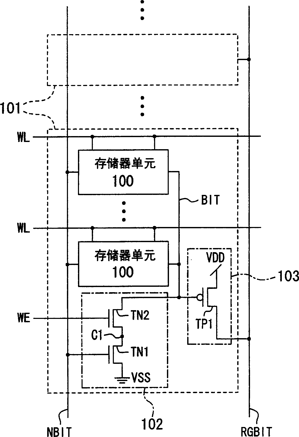
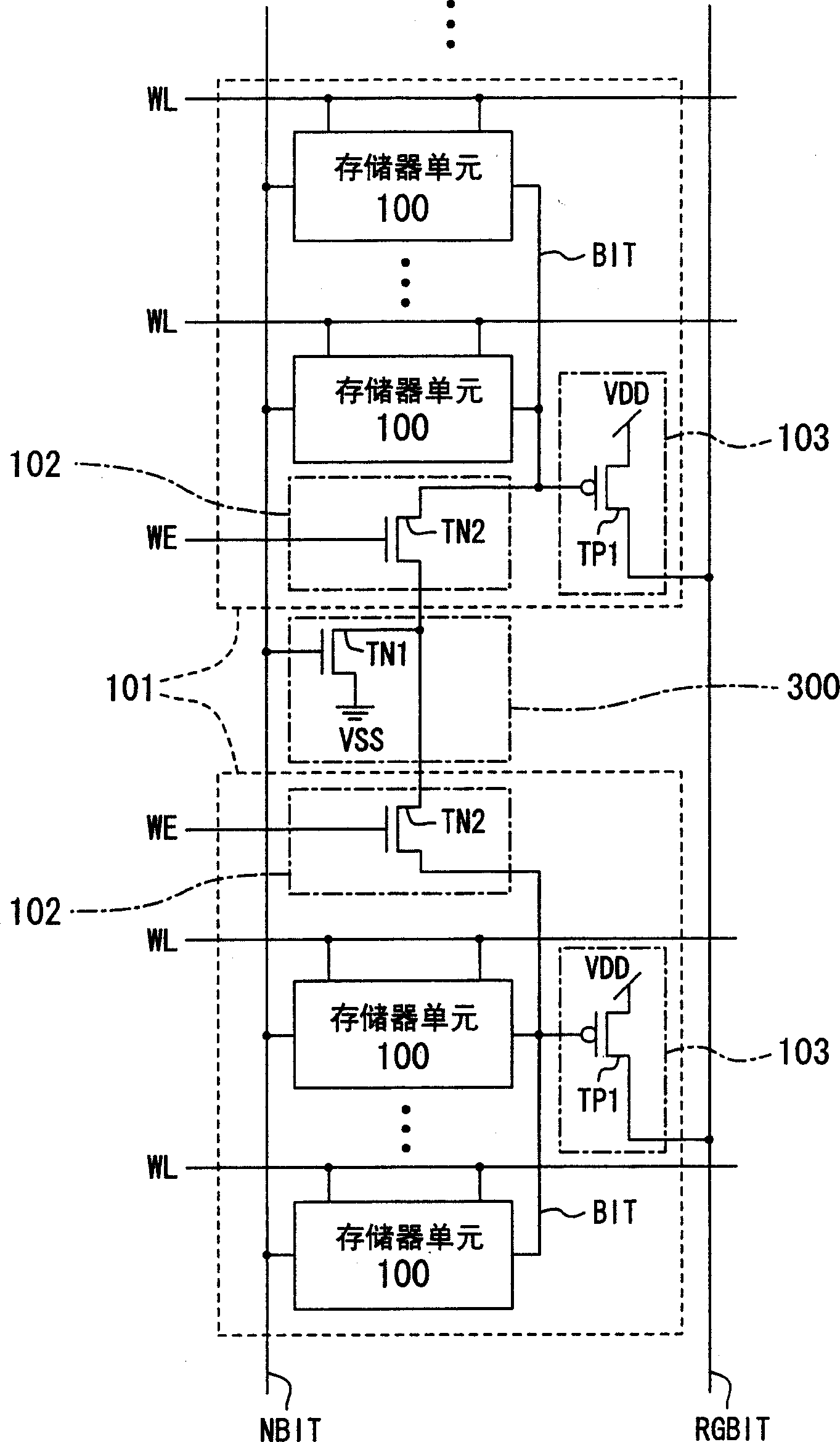
no. 3 approach
[0067] Figure 4The configuration of the semiconductor memory device according to the third embodiment of the present invention is shown.
[0068] In the same figure, a plurality of memory cells 100 are arranged in an array, and at least two or more memory cells 100 constitute a memory cell group 101 connected to the same bit line pair BIT, NBIT, and there are multiple memory cells in the bit line direction. Unit group 101. For a plurality of memory cell groups 101 arranged in the bit line direction, one bit line NBIT in the memory cell group 101 is commonly connected, and the other bit line BIT is connected to the global bit line RGBIT for readout via the readout unit 103 .
[0069] The P-type transistor TP1 provided in the above-mentioned readout portion 103 of each memory cell group 101 has its gate connected to the above-mentioned other bit line BIT, its source connected to a given power supply VDD, and its drain connected to the readout global The bit line RGBIT is conn...
PUM
 Abstract
Description
Claims
Application Information
 - R&D
- Intellectual Property
- Life Sciences
- Materials
- Tech Scout
- Unparalleled Data Quality
- Higher Quality Content
- 60% Fewer Hallucinations
Browse by: Latest US Patents, China's latest patents, Technical Efficacy Thesaurus, Application Domain, Technology Topic, Popular Technical Reports.
© 2025 PatSnap. All rights reserved.Legal|Privacy policy|Modern Slavery Act Transparency Statement|Sitemap|About US| Contact US: help@patsnap.com