Method for multibank memory scheduling
A storage bank, memory technology, applied in static memory, digital memory information, information storage and other directions, can solve problems such as complex logic circuits
- Summary
- Abstract
- Description
- Claims
- Application Information
AI Technical Summary
Problems solved by technology
Method used
Image
Examples
Embodiment Construction
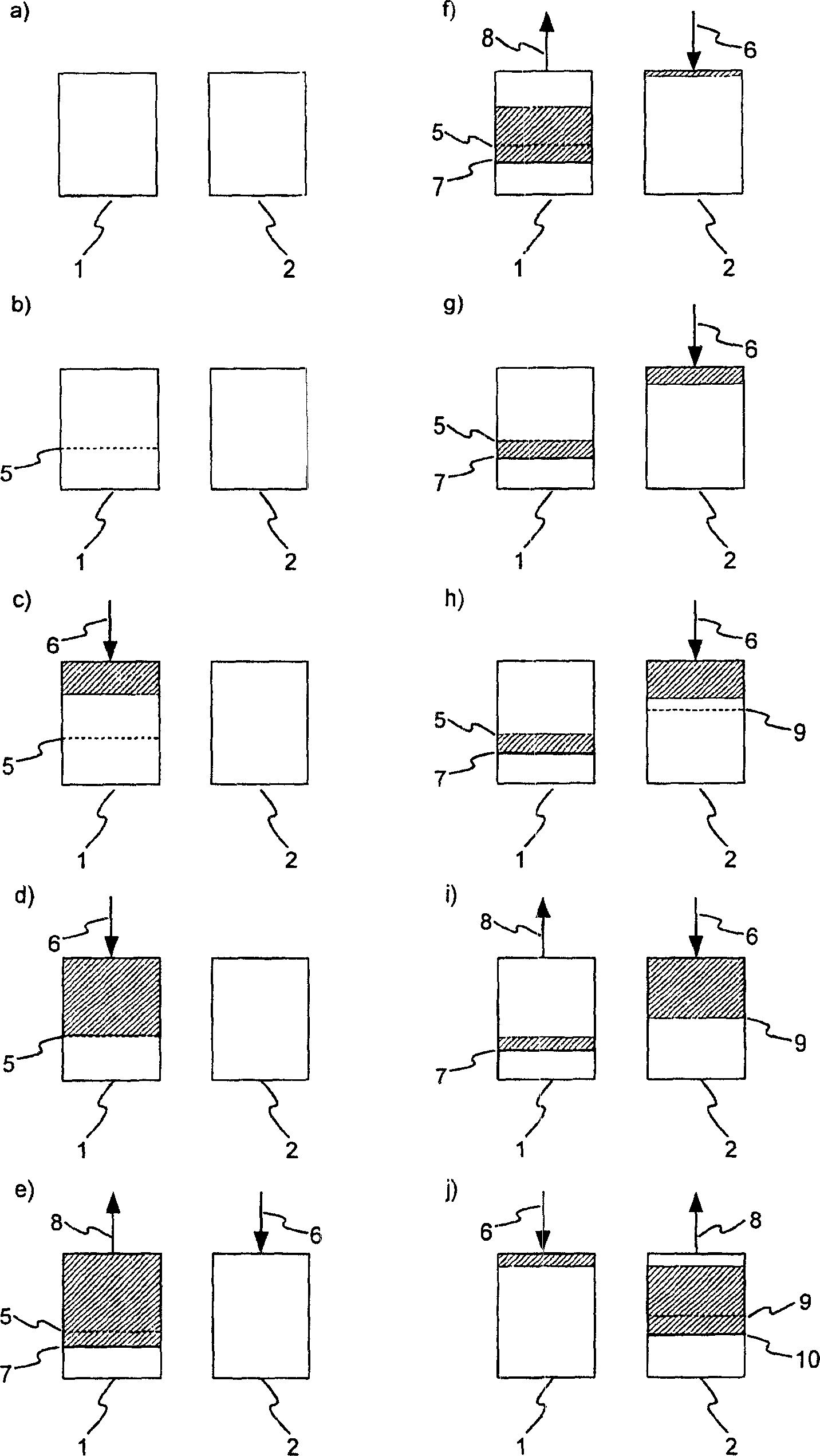
[0030] exist figure 1The access to the two memory banks 1, 2 of the SDRAM using the method according to the invention is shown in . For simplicity, accesses are divided into a sequence of states of the bank, which are in figure 1 Parts a) to j) of . For clarity, only a single complete output block is written to one bank 1,2 in the figure. Of course, multiple output blocks can be written to the memory bank sequentially. When the access starts, both banks 1 and 2 are empty, which corresponds to figure 1 a). As shown in part b), in the left bank 1, a pointer 5 is set to mark the size of the output block. The input stream 6 from the driver is now stored in left bank 1, which is shown in part c). The buffer can be read once pointer 5 is reached. Write operations to left bank 1 continue until a read access occurs. This is shown in part d). Thus, the first memory bank 1 is filled with a plurality of output blocks. After the first read access to left bank 1, the input stream...
PUM
 Abstract
Description
Claims
Application Information


