
In-plane switching liquid crystal display device

一种液晶显示装置、内切换的技术,应用在晶体管、静态指示器、光学等方向,能够解决降低孔径比等问题

Inactive Publication Date: 2005-04-20
LG DISPLAY CO LTD
View PDF0 Cites 21 Cited by
  • Summary
  • Abstract
  • Description
  • Claims
  • Application Information

AI Technical Summary

Problems solved by technology

However this reduces the aperture ratio

Method used


Image

  • In-plane switching liquid crystal display device
  • In-plane switching liquid crystal display device
  • In-plane switching liquid crystal display device

Examples


Embodiment Construction

[0036] Embodiments of the invention will now be described in detail, examples of which are illustrated in the accompanying drawings.

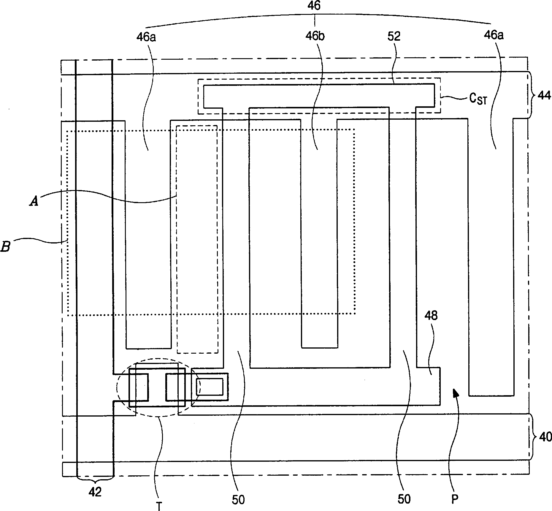
[0037] Figure 4 is a plan view of an array substrate for an in-plane switching liquid crystal display device according to a first embodiment of the present invention.

[0038] exist Figure 4 In this example, the gate line 110 is formed in a first direction, and the data line 126 is formed in a second direction. The gate lines 110 and the data lines 126 cross each other to define a pixel region P. Referring to FIG. Thin film transistors T are formed at intersections of the gate and data lines 110 and 126 . In the pixel region P, a plurality of pixel electrodes 130 connected to the thin film transistors T are formed. A plurality of common electrodes 118 are formed in the pixel region P, which are arranged in an alternate manner with the plurality of common electrodes 130 .

[0039] In the first embodiment, the pixel electrode 130 and the com...


PUM


Abstract

An in-plane switching liquid crystal display device. The invention discloses a substrate for an in-plane switching liquid crystal display device, comprising: a gate line along a first direction; a data line along a second direction, and the data line crosses the gate line to define A pixel area; a thin film transistor located at the intersection of the gate and data lines; a plurality of pixel electrodes located in the pixel area along the third direction, and the pixel electrodes are connected to the thin film transistor; There are multiple common electrodes in three directions, the common electrodes and the pixel electrodes are arranged alternately; and an alignment layer covering the common electrodes and the pixel electrodes, the alignment layer has an alignment along the first direction direction.

Description

technical field [0001] The present invention relates to liquid crystal display (LCD) devices, and more particularly, the present invention relates to in-plane switching liquid crystal display (IPS-LCD) devices. Background technique [0002] Liquid crystal display (LCD) devices have been considered as next-generation display devices of great value due to low power consumption and ease of portability. [0003] The optical anisotropy and polarization properties of liquid crystal materials are the basis for driving LCD devices. In general, an LCD device includes: two substrates arranged apart from each other and facing each other; and a liquid crystal layer interposed between the two substrates. Polarizing plates are respectively arranged on the outer surfaces of the two substrates. Each of the two substrates includes electrodes, and the electrodes of the two substrates also face each other. The voltage applied to each electrode creates an electric field between the electrode...

Claims


Application Information

Patent Timeline
Patent Type & Authority Applications(China)
IPC IPC(8): G02F1/1337G02F1/1343G02F1/1368
CPCG02F1/133784G02F1/134363G02F1/1337
Inventor 金度成姜炳求
Owner LG DISPLAY CO LTD
Features
  • Generate Ideas
  • Intellectual Property
  • Life Sciences
  • Materials
  • Tech Scout
  • Unparalleled Data Quality
  • Higher Quality Content
  • 60% Fewer Hallucinations
Learn More