
Patsnap Eureka
For R&D, Patsnap Eureka makes reading and utilizing patents & technical documents easy.
Patsnap Eureka AIR
Designed for self-driven R&D workflows. Generate viable solutions, solve complex R&D challenges, empower your innovation with AI.

Patsnap Eureka Materials
Designed for material experts only. Revolutionize your material R&D, from search, analyze, to developing new materials.

TechResearch
Generate reliable direction feasibility study reports for your R&D in just a few steps.

TechSeek
Discover and master advanced knowledge NOW. Basics, ideas, possibilities, all at once.

TechMind
As an expert in R&D Theories, TechMind can generates customized viable solutions instantly.

TechRisk
Analyze your overall solution with one click, know your potential R&D risks in advance.

TechMonitor
Get weekly tech updates, stay abreast of the latest tech innovations and key insights.
Thermal transfer element
一种热转移、元件的技术,应用在电气元件、电固体器件、半导体器件等方向,能够解决产量降低、厚度不规则等问题
- Summary
- Abstract
- Description
- Claims
- Application Information
AI Technical Summary
Problems solved by technology
Method used
Image

Examples
no. 1 example
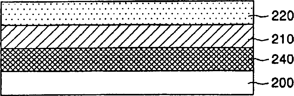
[0026] figure 2 is a cross-sectional view of a laser thermal transfer element for forming an organic thin film layer of an OLED according to a first embodiment of the present invention;
[0027] refer to figure 2 , The laser thermal transfer element according to the first embodiment of the present invention includes a base substrate 200 , a light-to-heat conversion (LTHC) layer 210 , and a transfer layer 220 . The base substrate 200 serves as a supporting substrate for supporting the laser thermal transfer element. The base substrate 200 is made of a transparent polymer such as polyester, polypropylene, polyepoxy, polyethylene, polystyrene, polyethylene terephthalate, etc., and has a thickness of about 10-500Φm. The base substrate 200 may employ a substrate such as a glass substrate or a thin film.
[0028] The LTHC layer 210 absorbs light to convert light into thermal energy, and it has a suitable optical density and includes a light absorbing material. The light-absorb...
PUM
 Abstract
Description
Claims
Application Information
 - R&D Engineer
- R&D Manager
- IP Professional
- Industry Leading Data Capabilities
- Powerful AI technology
- Patent DNA Extraction
Browse by: Latest US Patents, China's latest patents, Technical Efficacy Thesaurus, Application Domain, Technology Topic, Popular Technical Reports.
© 2024 PatSnap. All rights reserved.Legal|Privacy policy|Modern Slavery Act Transparency Statement|Sitemap|About US| Contact US: help@patsnap.com