Structure of forming pressure contact with power semiconductor module

A technology of power semiconductor and connection structure, applied in the direction of semiconductor device, printed circuit structure connection, semiconductor/solid-state device components, etc., can solve the problem of not guaranteeing the reliability of welding connection and contact

Inactive Publication Date: 2005-11-23
SEMIKRON ELECTRONICS GMBH & CO KG
View PDF3 Cites 16 Cited by
  • Summary
  • Abstract
  • Description
  • Claims
  • Application Information

AI Technical Summary

Problems solved by technology

[0006] The disadvantage of this power semiconductor module structure is that two different joining processes are required to integrate the module into a mounting structure (screw connection and soldering, which have to be carried out in several steps)
A major disadvantage is that the contact reliability of soldered connections cannot be guaranteed over a long period of use

Method used


Image

  • Structure of forming pressure contact with power semiconductor module
  • Structure of forming pressure contact with power semiconductor module
  • Structure of forming pressure contact with power semiconductor module

Examples


Embodiment Construction

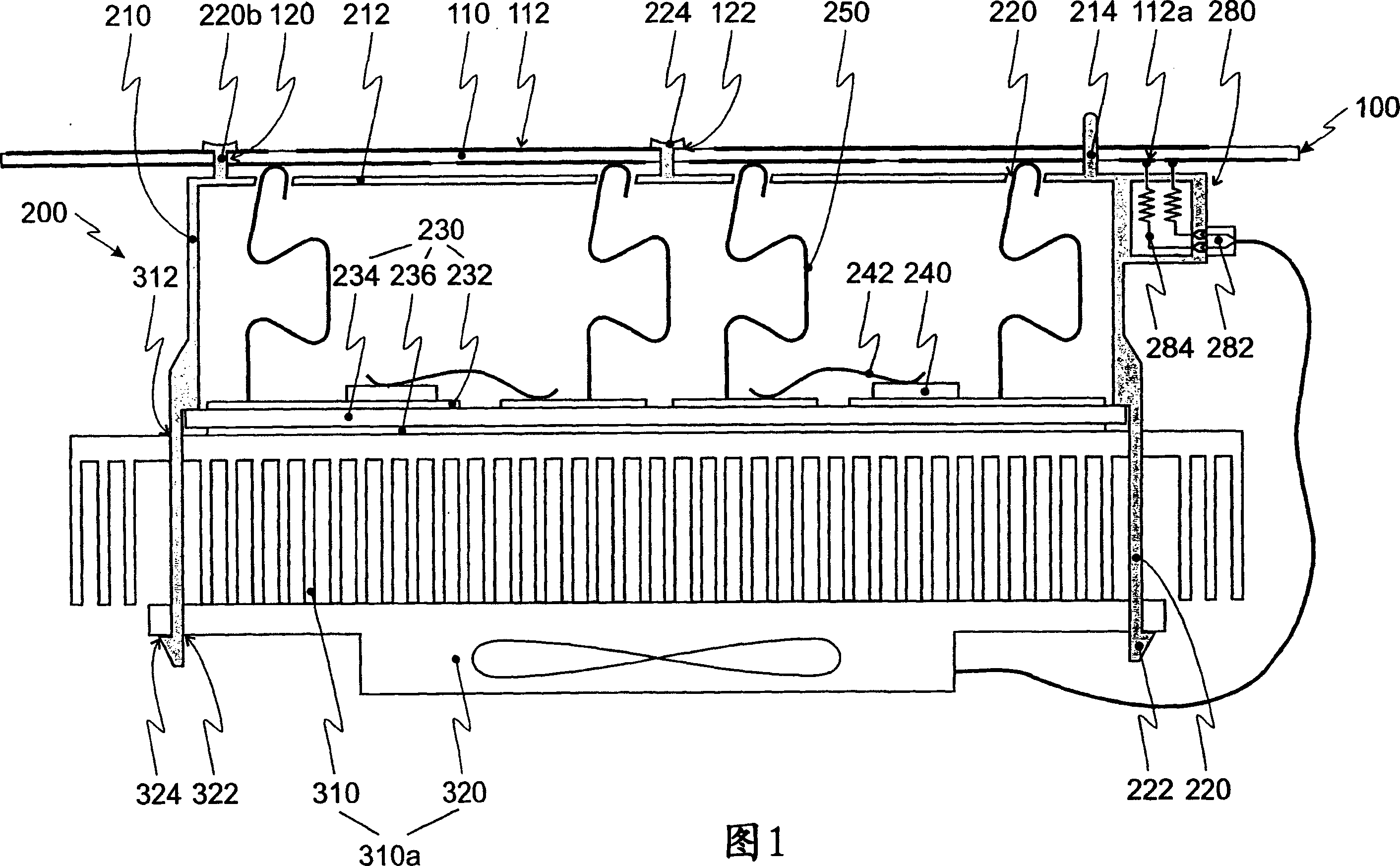
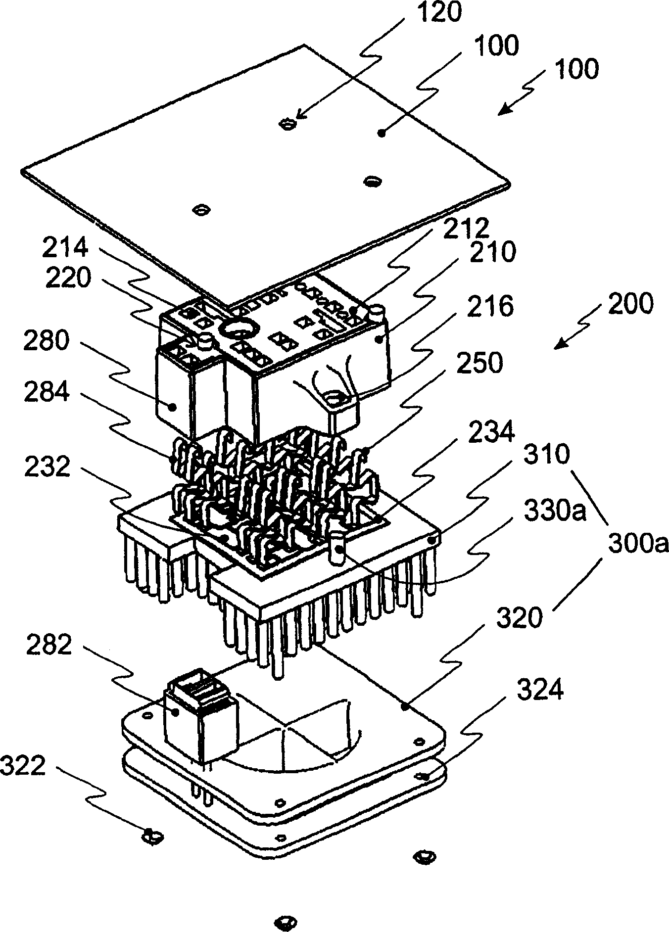
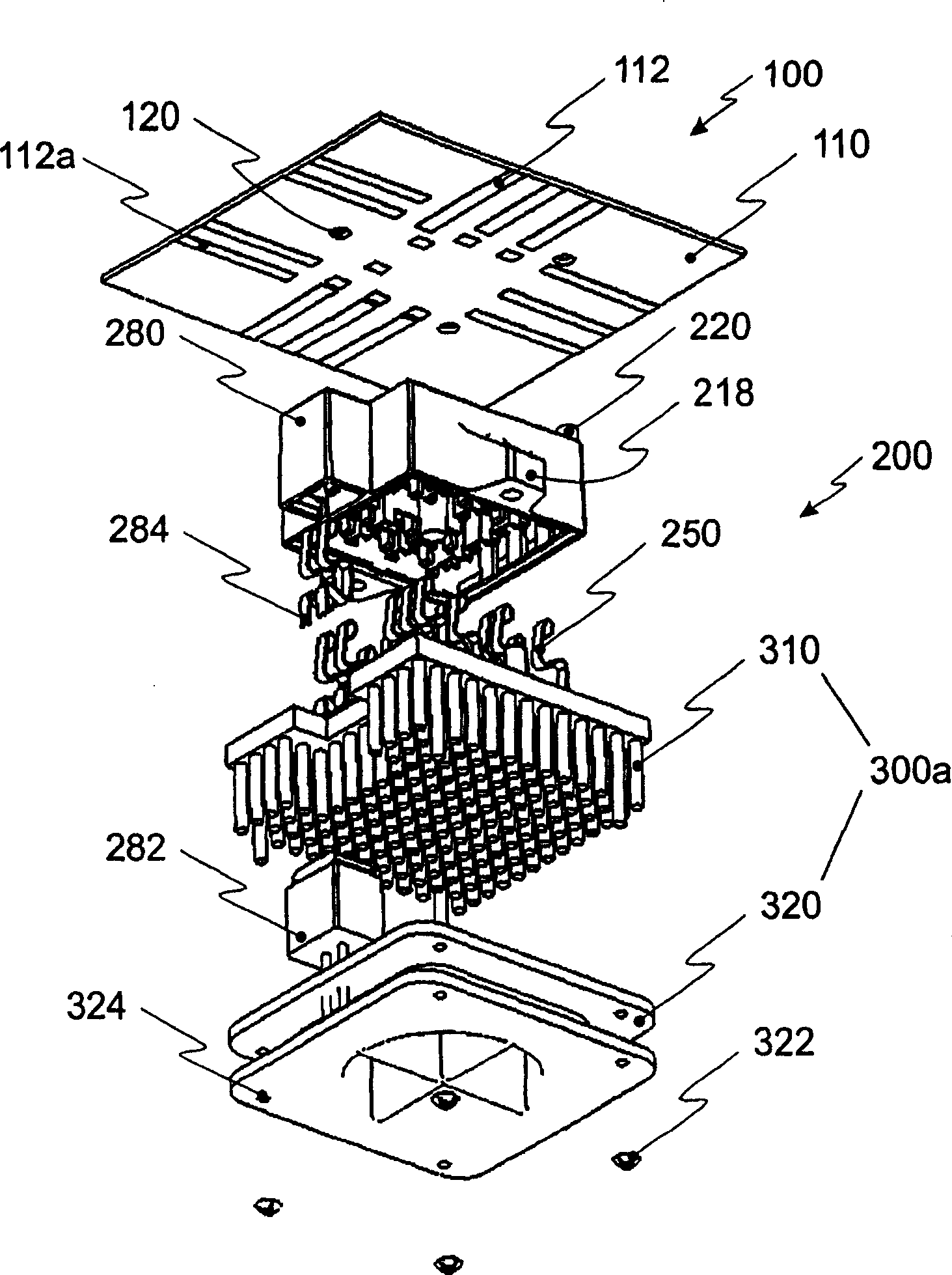
[0025] Figure 1 shows a cross-section of the structure of the present invention. The structure shown consists of a circuit board 100 , a power semiconductor module 200 and a cooling device 300 .

[0026] The circuit board 100 has an insulator 110, and conductive strips 112 arranged on and / or within the insulator. These busbars carry signals such as load signals, control signals and auxiliary signals of the power semiconductor module 200 .

[0027] The power semiconductor module 200 has a frame-like housing 210 with an integrated cover 212 . The second cover of the housing 210 is constituted by the base plate 230 . The substrate consists of an insulator 234, preferably a technical ceramic such as aluminum oxide or aluminum nitrite, and metal layers 232, 236 on both sides of the insulator. Here the metal layer is applied on the insulator 234 by means of the known DCB method. Preferably, the metal layer 232 towards the interior of the housing is structured to form mutually in...


PUM


Abstract

Power semiconductor module with a pressure contact comprises circuit board (100), cooling body (300b) and a semiconductor power module (200) with an insulated plastic housing (210) and cover (212) with recesses. A second cover has a substrate (230) with semiconductor elements (240) and contact spring connections with reversible or permanent connections.

Description

technical field [0001] The present invention describes a structure that makes pressure contact with a very compact power semiconductor module. DE 19630173 C2 or DE 19924993 C2 discloses a modern design of such a power semiconductor module with high power relative to its size, which is the starting point of the present invention. Background technique [0002] DE19630173C2 discloses a power semiconductor module for direct mounting on a cooling device, which consists of a housing and an electrically insulating base plate, the base plate being an insulating material body with a plurality of mutually insulated metal conductive strips thereon and an insulating material body located on the insulating Power semiconductor components on a body of material and in circuit connection with these conductive strips. The external electrical connection to the busbars of the circuit board outside the housing is made by means of contact springs. [0003] The power semiconductor module also ha...

Claims


Application Information

Patent Timeline
Patent Type & Authority Applications(China)
IPC IPC(8): H01L23/34H01L23/36H01L23/40H01L23/48H01L25/07H01L25/16H05K1/03H05K1/14H05K3/32
CPCH01L2924/01013H05K1/141H01L2924/01033H01L2924/01082H01L24/48H01L25/072H05K1/0306H01L2224/48472H01L2224/48091H01L2924/13055H05K2201/0311H01L2924/19041H01L24/72H05K3/325H01L2924/19043H01L23/4093H01L2924/14H05K2201/10757H01L25/162H01L2924/13091H01L2924/00014H01L2924/00H01L2224/45099H01L2224/45015H01L2924/207
Inventor 莱纳·波普马可·莱德霍尔克里斯蒂·格布尔托马斯·施托克迈尔
Owner SEMIKRON ELECTRONICS GMBH & CO KG
Why Eureka
Try Eureka