Light emitting device and lighting device

A technology of light-emitting devices and light-emitting elements, which is applied in the direction of lighting devices, lighting and heating equipment, semiconductor devices of light-emitting elements, etc., which can solve problems such as the difficulty in improving the intensity and brightness of light emitted by light-emitting devices, and the attenuation of reflected light intensity, so as to improve the emission The effect of high light intensity, brightness and luminous efficiency

Inactive Publication Date: 2006-01-04
KYOCERA CORP
View PDF1 Cites 21 Cited by
  • Summary
  • Abstract
  • Description
  • Claims
  • Application Information

AI Technical Summary

Problems solved by technology

However, the energy of the light that is repeatedly reflected and passes through the wavelength conversion layer 15 multiple times is absorbed, and the intensity of the reflected light is attenuated.
[0013] As described above, in conventional light emitting devices, it is difficult to increase the intensity and brightness of emitted light from the light emitting device.

Method used


Image

  • Light emitting device and lighting device
  • Light emitting device and lighting device
  • Light emitting device and lighting device

Examples


Embodiment 1

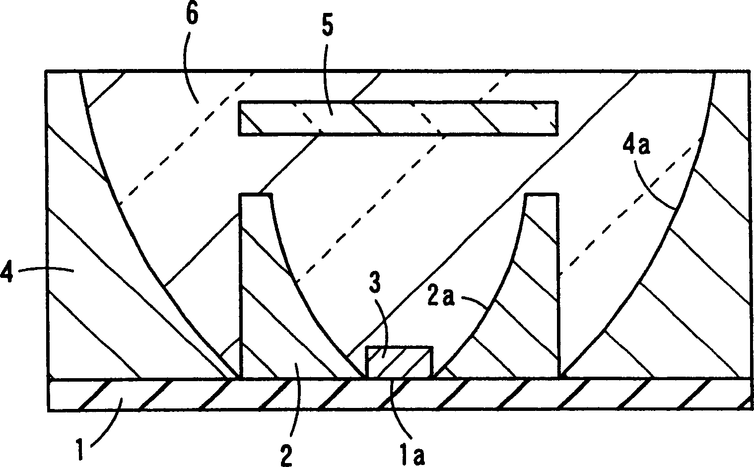
[0165] For the light-emitting device of the present invention, examples will be shown below. First, a base 1 made of alumina ceramics to be the base 1 was prepared. Moreover, substrate 1 such as image 3 As shown, it is integrally formed so that the placement portion 1a protrudes, and the upper surface of the placement portion 1a is parallel to the upper surface of the base body 1 other than the placement portion 1a.

[0166] The base 1 is a member in which a cuboid mounting part 1a of width 0.35 mm x depth 0.35 mm x thickness 0.15 mm is formed on the upper central part of a cuboid of width 17 mm x depth 17 mm x thickness 0.5 mm.

[0167] In addition, a wiring conductor for electrically connecting the light emitting element 3 and the external circuit board via internal wiring formed inside the base body 1 is formed at the portion where the light emitting element 3 is mounted on the placement portion 1a. The wiring conductor is made of a metallization layer made of Mo-Mn powd...

Embodiment 2

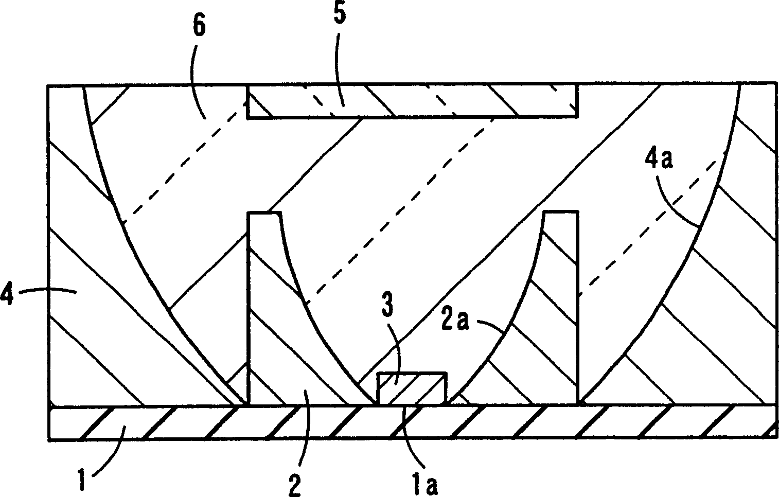
[0187] For the light-emitting device of the present invention, examples will be shown below. First, a substrate 1 made of alumina ceramics to be a substrate 1 was prepared. Moreover, substrate 1 such as Figure 16 As shown, it is integrally formed so that the placement portion 1a protrudes, and the upper surface of the placement portion 1a is parallel to the upper surface of the base body 1 other than the placement portion 1a.

[0188] The base 1 is a member in which a cuboid mounting part 1a of width 0.35 mm x depth 0.35 mm x thickness 0.15 mm is formed on the upper central part of a cuboid of width 17 mm x depth 17 mm x thickness 0.5 mm.

[0189] In addition, a wiring conductor for electrically connecting the light emitting element 3 and the external circuit board via internal wiring formed inside the base body 1 is formed at the portion where the light emitting element 3 is mounted on the placement portion 1a. The wiring conductor is made of a metallization layer made of ...


PUM


Abstract

The invention provides a light-emitting device which is equipped with: a light-emitting element (3); a matrix (1) which is equipped with a placement part (1a) for placing the light-emitting element (3) on the upper main surface; a first frame-shaped reflective component (2) which is formed on the upper main surface of the matrix (1) according to a way of surrounding the placement part (1a); a second frame-shaped reflective component (4) which is formed on the upper main surface of the matrix (1) according to a way of surrounding the first reflective component (2); a light transmittance component (6) which is arranged on the inner lateral of the second reflective component (4) according to a way of covering the light-emitting element (3) and the first reflective component (2); a first wavelength conversion layer (5) which is arranged in the inside of the light transmittance component (6) on the upper part of the light-emitting element (3) with intervals to the first and the second reflective components (2, 4) and converts the wavelength of lights that are sent out from the light-emitting element (3).

Description

technical field [0001] The present invention relates to a light-emitting device incorporating a light-emitting element and a lighting device using the light-emitting device. Background technique [0002] Figure 15 shows a conventional light-emitting device. Figure 15 Among them, the light-emitting device is mainly composed of a substrate 11 , a frame-shaped reflective member 12 , a light-emitting element 13 , a wavelength conversion layer 15 , and a light-transmitting member 16 . The substrate 11 is made of an insulator, and has a placement part 11a for placing the light-emitting element 13 in the central part of the upper surface, and is formed with a lead terminal and a metallization arrangement that electrically connects the inside and outside of the light-emitting device from the placement part 11a and its periphery. Wiring conductors (not shown) composed of wires and the like. The frame-shaped reflective member 12 is adhesively fixed on the upper surface of the base ...

Claims


Application Information

Patent Timeline
Patent Type & Authority Applications(China)
IPC IPC(8): H01L33/00F21S2/00F21K99/00H01L33/50H01L33/60
CPCH01L33/507H01L33/60F21Y2105/10F21Y2115/10H01L2224/48091H01L2924/00014
Inventor 松浦真吾关根史明
Owner KYOCERA CORP
Why Eureka
Try Eureka