Stereo-stacking packaging structure

A packaging structure and stacking technology, applied in the direction of electric solid-state devices, semiconductor devices, semiconductor/solid-state device components, etc., can solve problems such as production difficulties and unstable yields, and achieve the effects of improving reliability and facilitating production

Active Publication Date: 2006-03-01
IND TECH RES INST
View PDF2 Cites 6 Cited by
  • Summary
  • Abstract
  • Description
  • Claims
  • Application Information

AI Technical Summary

Problems solved by technology

However, this packaging structure can only be electrically tested after all the chips are stacked. Therefore, if any chip has a problem during the stacking process, the package structure completed by the entire stack cannot be used, making the yield unstable. and cause difficulties in production

Method used


Image

  • Stereo-stacking packaging structure
  • Stereo-stacking packaging structure
  • Stereo-stacking packaging structure

Examples


Embodiment Construction

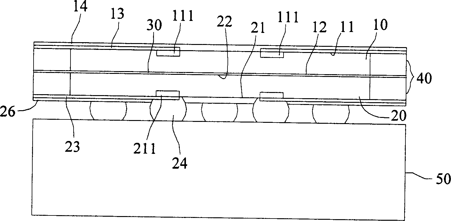
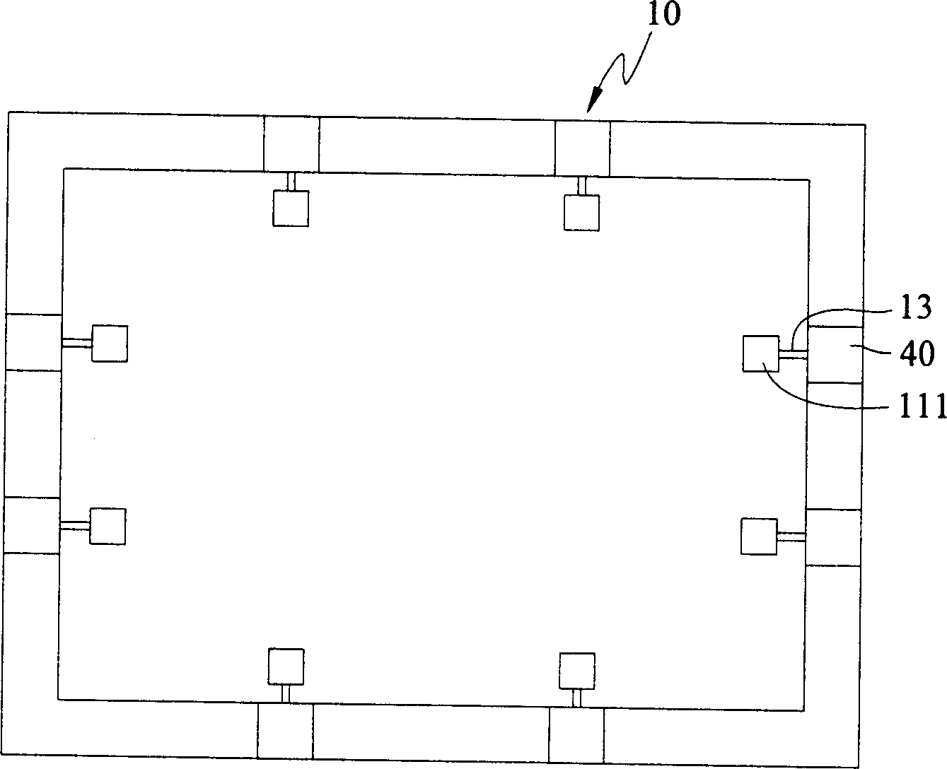
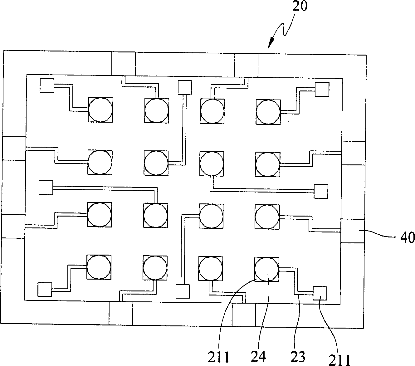
[0056] Please refer to figure 1 As shown, it is a cross-sectional view of the first embodiment of the three-dimensional stacked packaging structure of the present invention; please refer to Figure 2A and Figure 2B As shown in FIG. 2 , they are schematic diagrams of the upper surfaces of the first component 10 and the second component 20 in the first embodiment, respectively.

[0057] In this packaging structure, a first component 10 and a second component 20 are stacked together in a back-to-back manner, and the metal pads on the first component 10 and the second component 20 are used as input / output ports by using the circuit redistribution technology. Pull it to the edge of the first element 10 and the second element 20 , and make it electrically connected up and down, and then transmit the signal with the printed circuit board 50 through the conductive bump 24 on the second element 20 .

[0058]The first component 10 and the second component 20 can be: chip-to-chip bond...


PUM


Abstract

A stereo - stack type of packaging structure is prepared as stacking the first and the second elements back to back together , utilizing the rewiring technique to span - wire metal pads the first and the second element surface to edges of the first and the second elements , using a conductive column to connect through electricity of top and bottom for carrying out signal transmission between two elements , then utilizing conductive lug on the second element and printed circuit to carry out signal transmission .

Description

technical field [0001] The invention relates to a three-dimensional stack packaging structure, in particular to a three-dimensional stack packaging structure formed by joining two components in a back-to-back manner. Background technique [0002] Electronic packaging (Electronic Packaging) is also known as electronic packaging, and its purpose is to give integrated circuit components (IC) an organizational structure so that they can perform their intended functions. From the perspective of the processing of microelectronic products, electronic packaging belongs to the processing technology of the back end of the product, so structure is often considered to be only one of the supporting roles of integrated circuit processing technology. In fact, electronic packaging technology dominates the size and cost of electronic products, so the development of packaging technology is as important as IC processing technology and other microelectronics-related processing technologies. ...

Claims


Application Information

Patent Timeline
Patent Type & Authority Applications(China)
IPC IPC(8): H01L25/00H01L23/00
CPCH01L2224/11
Inventor 张恕铭何宗哲
Owner IND TECH RES INST
Why Eureka
Try Eureka