Apparatus and method for single die backside probing of semiconductor devices
一种半导体、器件的技术,应用在单晶粒背面探测的装置领域
- Summary
- Abstract
- Description
- Claims
- Application Information
AI Technical Summary
Problems solved by technology
Method used
Image

Examples
Embodiment Construction
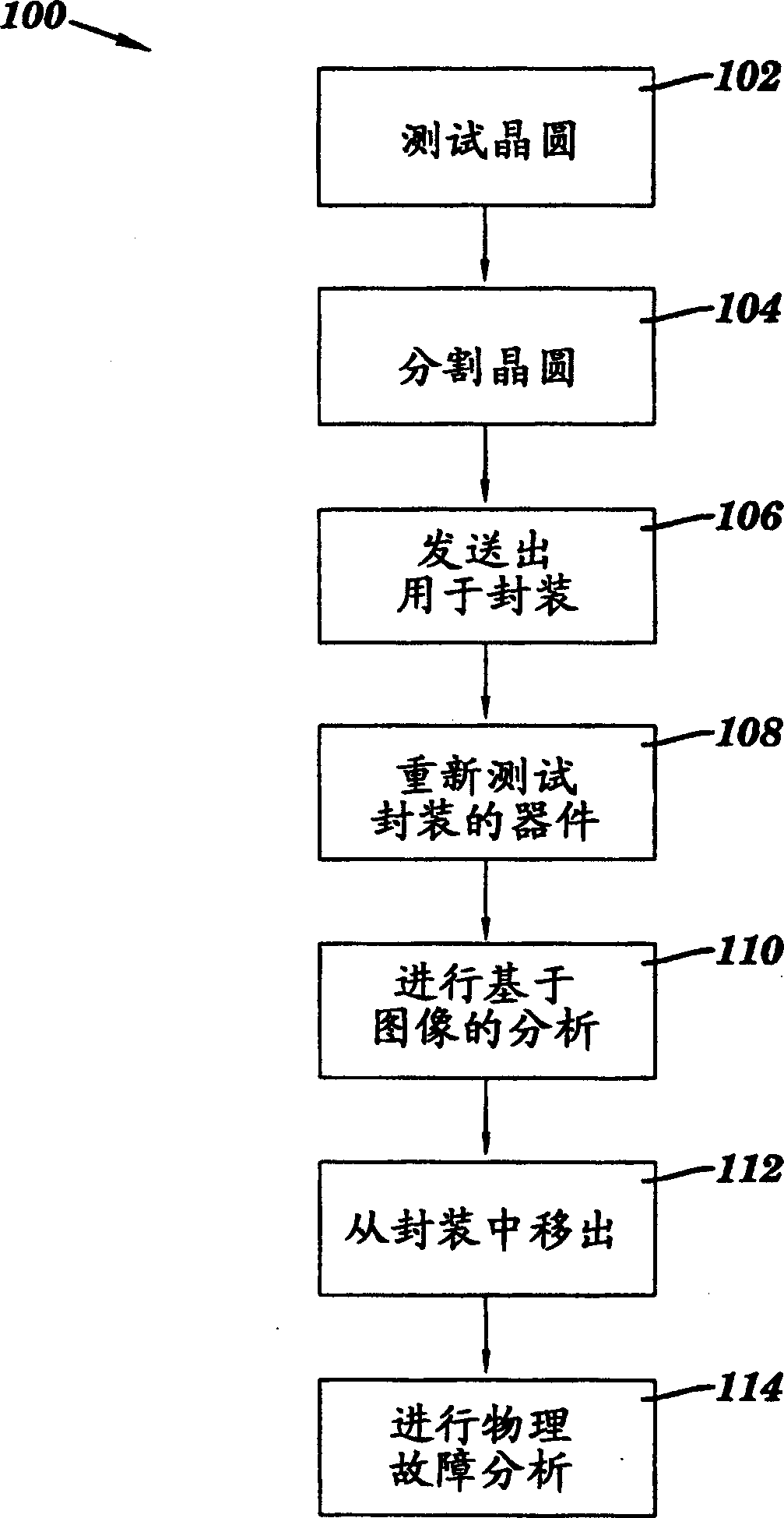
[0024] Disclosed herein are apparatus and methods for single die backside probing of semiconductor devices that allow for single die backside analysis using currently available cantilever probe cards. The apparatus can also be adapted for use with optical microscopes (e.g., available from Hypervision, Inc. and A microscope obtained from Hamamatsu Corporation) was used in combination. While existing systems are suitable for full wafer backside probing, there is currently no device as suitable for single die probing as the embodiments of the present invention described below.
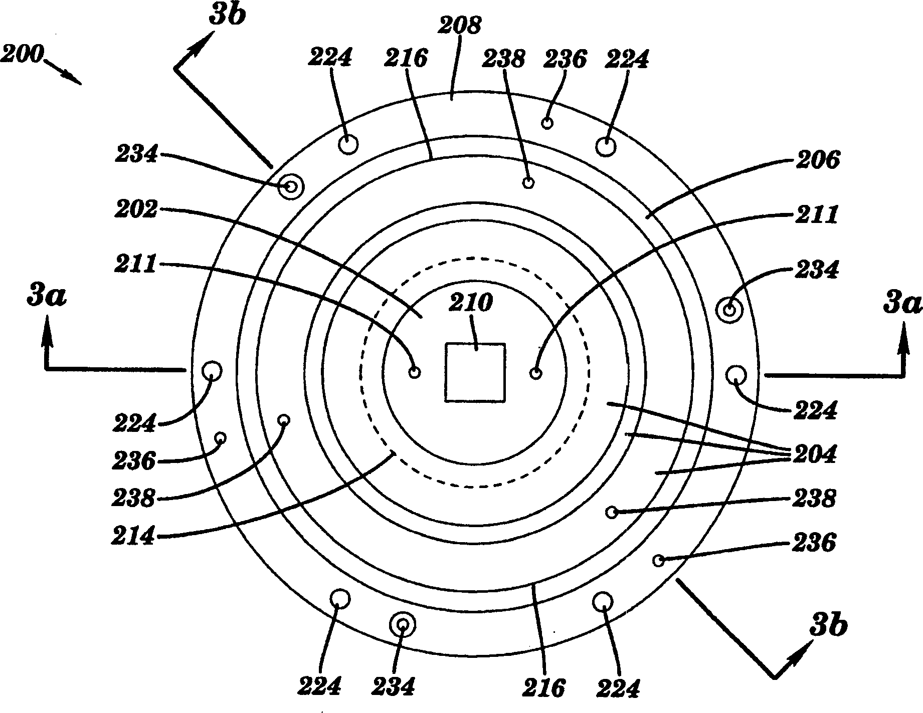
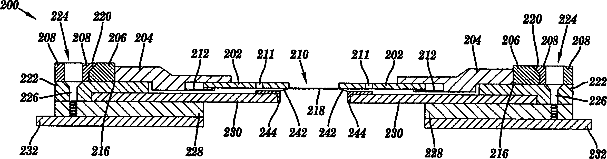
[0025] Briefly, an embodiment of the device includes a mechanism to accommodate a cantilevered probe card, a mechanical mount to perform "Z" height adjustment, and a plate with a hole in the center to support the crystal to be inspected. grain. The grain to be analyzed is placed on the cantilever probe card in an inverted position so that it can be inspected using an optical microscope. An advantage of...
PUM
 Abstract
Description
Claims
Application Information
 - R&D
- Intellectual Property
- Life Sciences
- Materials
- Tech Scout
- Unparalleled Data Quality
- Higher Quality Content
- 60% Fewer Hallucinations
Browse by: Latest US Patents, China's latest patents, Technical Efficacy Thesaurus, Application Domain, Technology Topic, Popular Technical Reports.
© 2025 PatSnap. All rights reserved.Legal|Privacy policy|Modern Slavery Act Transparency Statement|Sitemap|About US| Contact US: help@patsnap.com