Image display apparatus
一种图像显示设备、显示设备的技术,应用在图像/图形显示管、静态指示器、放电管冷阴极等方向,能够解决电子入射位置不同、亮度和颜色偏差、密闭容器翘曲等问题
- Summary
- Abstract
- Description
- Claims
- Application Information
AI Technical Summary
Problems solved by technology
Method used
Image

Examples
Embodiment 1
[0060] Embodiments of the image display device of the present invention are described.
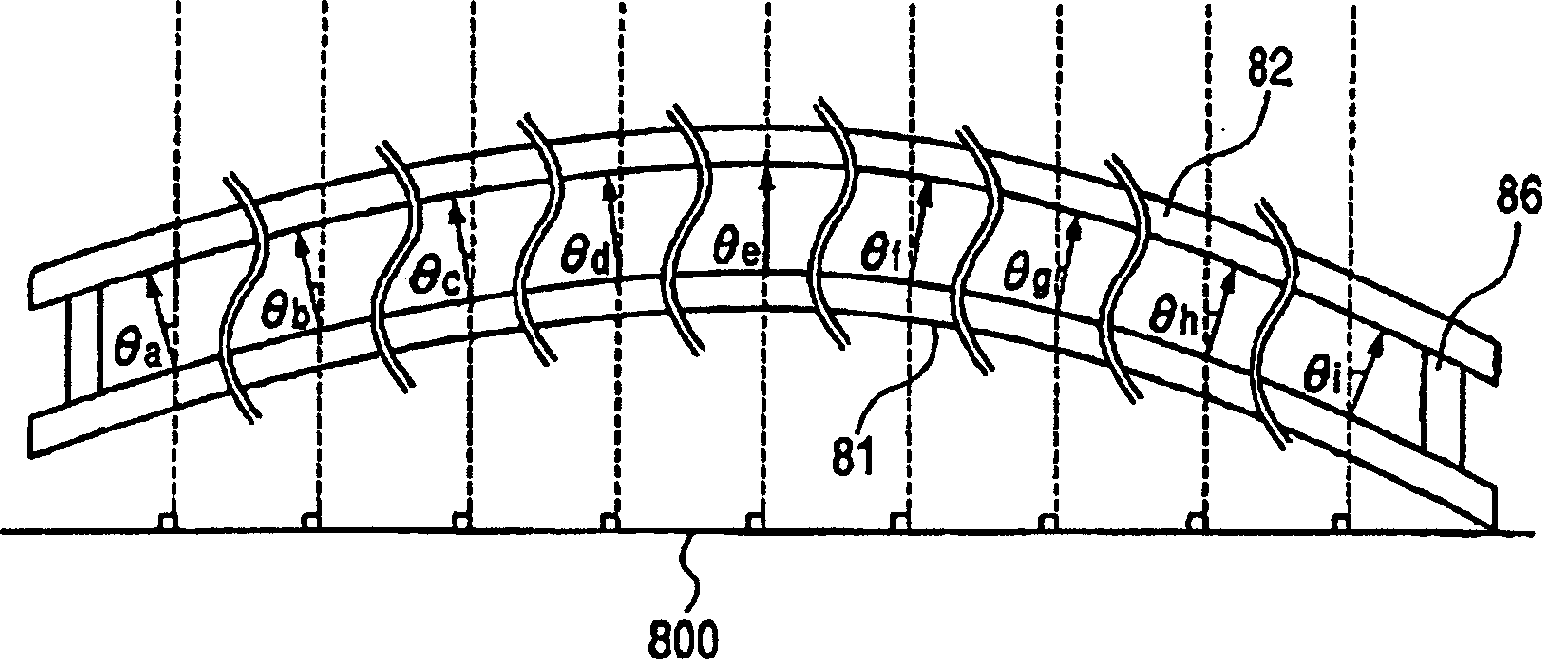
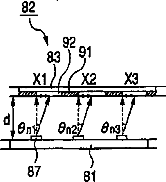
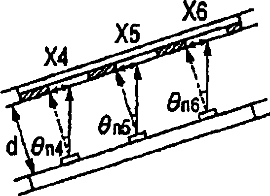
[0061] image 3 is a perspective view of an image display device. A portion of the device is cut away in order to show its internal structure. An enlarged sectional view of the sealed connection is shown in the lower dotted line. in accordance with image 3 , the image display device of the present embodiment has a housing 90 including a rear panel 81, a front panel 82 arranged opposite to the rear panel 81, and a bracket 86 supporting these panels. Many electron-emitting devices 87, which are surface-conduction electron-emitting devices here, are arranged in a matrix on the rear plate 81, and a pair of device electrodes in each of these surface-conduction electron-emitting devices 87 are respectively connected to Wire 88 and wire 89 in the Y direction. In the current embodiment, the X direction is the same as the horizontal (column) direction, and the Y direction is the same as the v...
Embodiment 2
[0087] The current embodiment is where such as Figure 12 The electrode shape shown is the case of an arc, and other structures in the present embodiment are the same as those in Embodiment 1. In this case, if, as described in Example 1, in the Y direction, in the Figure 12 Electron emission regions are formed at predetermined angular positions dy4-dy6 on the electrodes of Y4-Y6, and the initial velocity vector of the electron beam can be arbitrarily selected. That is, by forming the in-plane distribution at the position of the electron emission region, the electron beam incident position is brought to the correct position. Figure 13 is a graph showing the relationship between the angle between the reference plane and the normal and the shift of the position of the corresponding electron-emitting region in the case where the electrode radius Ry is 100 μm. By the method similar to Example 1, make Figure 13 China's relationship with Figure 9 Corresponding to the position...
Embodiment 3
[0089] In the current embodiment, the electrode angle is zero degrees over the entire surface of the image display device (opposite portions of a pair of device electrodes are parallel to the wires in the Y direction). However, the current embodiment brings the electron beam incident position to the correct position on the front plate by forming the in-plane distribution in the electron beam steering effect due to the matrix structure. The current embodiment will be described in detail below.
[0090] The rigid structure of the wire in the Y direction affects the horizontal electron incident distance dx of the electron beam. The main parameters of the wire in the Y direction are the distance xd from the electron source, and the wire height hd in the Y direction, and these parameters will affect the electron orbit. use Figure 17 To be specific, when the distance xd becomes smaller, the orbit of the electron beam changes from dx4 to dx3, for example, as if it pushes away the ...
PUM
 Abstract
Description
Claims
Application Information
 - R&D
- Intellectual Property
- Life Sciences
- Materials
- Tech Scout
- Unparalleled Data Quality
- Higher Quality Content
- 60% Fewer Hallucinations
Browse by: Latest US Patents, China's latest patents, Technical Efficacy Thesaurus, Application Domain, Technology Topic, Popular Technical Reports.
© 2025 PatSnap. All rights reserved.Legal|Privacy policy|Modern Slavery Act Transparency Statement|Sitemap|About US| Contact US: help@patsnap.com