Laminated semiconductor device

A semiconductor and stacked technology, applied in the direction of semiconductor devices, semiconductor/solid-state device components, electric solid-state devices, etc., can solve the problems of inability to expand the size of semiconductor chips and decrease wiring efficiency, and achieve improved wiring efficiency and space utilization efficiency. Effect of Improving Noise Resistance Characteristics

Inactive Publication Date: 2006-10-11
PS4 LUXCO SARL
View PDF2 Cites 16 Cited by
  • Summary
  • Abstract
  • Description
  • Claims
  • Application Information

AI Technical Summary

Problems solved by technology

Therefore, there is a problem that the wiring efficiency decreases due to the interposer substrate, and the size of the semiconductor chip cannot be enlarged due to the restriction on the size of the bottom substrate.

Method used


Image

  • Laminated semiconductor device
  • Laminated semiconductor device
  • Laminated semiconductor device

Examples


Embodiment Construction

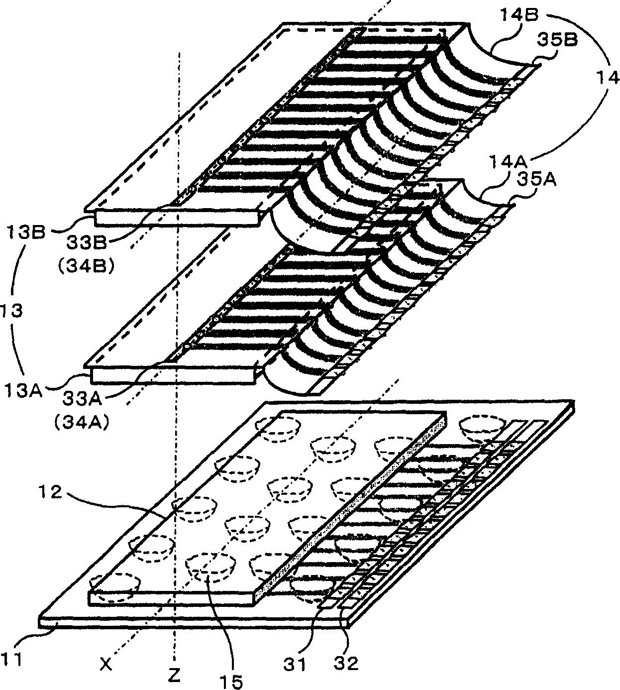
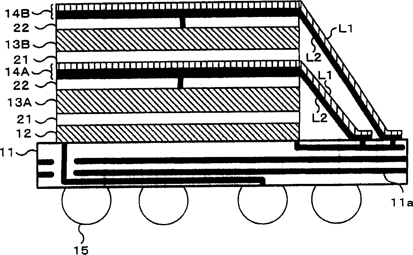
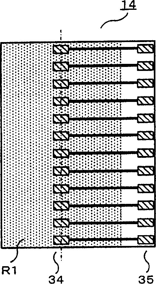
[0042]Embodiments of the present invention will be described below with reference to the drawings. In this embodiment, as an example of a stacked semiconductor device to which the present invention is applied, an embodiment in which a stacked memory is formed by stacking a plurality of DRAM chips will be described. Here, two examples in which the number of stacked DRAM chips are different for the stacked memory of this embodiment will be described. First, as a first embodiment, the basic structure of a stacked memory formed by stacking two DRAM chips will be described. As a diagram illustrating the structure of the stacked memory of the first embodiment, figure 1 is its exploded perspective view, and figure 2 is its cross-sectional structure diagram.

[0043] Such as figure 1 and figure 2 As shown, the stacked memory of the first embodiment has a structure in which three semiconductor chips are stacked on a base substrate 11 . The stacked three semiconductor chips incl...


PUM


Abstract

A stacked type semiconductor device comprising: a baseboard having a terminal row formed at an end in which connecting terminals is arranged linearly and having a wiring pattern connected to the connecting terminals and external terminals; semiconductor chips having a pad row in which pads is arranged linearly in parallel to the terminal row and being stacked on the baseboard; and interposer boards having a wiring layer including a plurality of wires arranged in parallel with the same length for connecting between pads of the pad row and connecting terminals of the terminal row.

Description

technical field [0001] The present invention relates to a stacked semiconductor device having a structure in which a plurality of semiconductor chips are stacked. Background technique [0002] In recent years, semiconductor memories such as DRAM (Dynamic Random Access Memory) have been required to have larger capacities in order to achieve higher functionality of devices. The larger the capacity of a semiconductor memory formed on one semiconductor chip, the more microfabrication is required, and thus the possibility of a decrease in yield is higher. Therefore, there have been proposals for a stacked semiconductor device having a structure in which a plurality of semiconductor chips are stacked on a base substrate. For example, by stacking a plurality of DRAM chips and an interface chip for controlling data input and output of each DRAM chip on a base substrate, a small and large-capacity stacked semiconductor device that can be controlled externally can be realized like a ...

Claims


Application Information

Patent Timeline
Patent Type & Authority Applications(China)
IPC IPC(8): H01L25/065H01L23/488
CPCH01L2924/01033H01L2924/01005H01L2924/01023H01L2924/15311H01L2924/01006H01L25/0657H01L2924/01082H01L2924/3011H01L24/50H01L2225/06579H01L2225/06551H01L2225/06527A01D23/04
Inventor 片桐光昭柴本正训原敦青木孝一郎谏田尚哉菊地修司谷江尚史
Owner PS4 LUXCO SARL
Why Eureka
Try Eureka