Semiconductor packing process

A packaging process and semiconductor technology, applied in the direction of semiconductor devices, semiconductor/solid device manufacturing, semiconductor/solid device components, etc., can solve problems such as limited, product scrapping, inconvenience, etc.

Active Publication Date: 2006-11-01
ADVANCED SEMICON ENG INC
View PDF0 Cites 1 Cited by
  • Summary
  • Abstract
  • Description
  • Claims
  • Application Information

AI Technical Summary

Problems solved by technology

[0002] Packages that use lead frames as substrates, such as quad flat no lead (QFN) packages, are often assembled on printed circuits by surface mount technology due to the excessive contact area on the lead frame. Large, it is difficult to control the amount of solder paste, and the defect of solder paste overflowing between the above-mentioned contacts and bridging occurs
If the situation is mild, it must be reworked; if the situation is serious, the product must be scrapped, resulting in a serious loss of output and yield
However, limited by the manufacturing process of the lead frame itself, even if the size of the above-mentioned contacts is reduced to the li

Method used


Image

  • Semiconductor packing process
  • Semiconductor packing process
  • Semiconductor packing process

Examples


Embodiment Construction

[0047] In order to further explain the technical means and effects that the present invention takes to achieve the intended purpose of the invention, the specific implementation methods, methods, steps, features and features of the semiconductor packaging process proposed according to the present invention will be described below in conjunction with the accompanying drawings and preferred embodiments. Efficacy, detailed as follows.

[0048] Figures 1A-1H Shown are a series of cross-sectional views showing the semiconductor packaging manufacturing process of the first embodiment of the present invention.

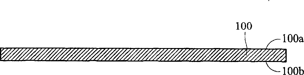
[0049] First, see Figure 1A As shown, a conductive substrate 100, preferably copper or aluminum, is provided. The conductive substrate 100 has opposite first surface 100a and second surface 100b.

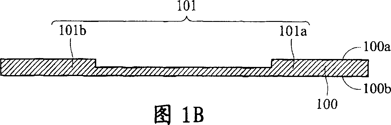
[0050] Next, as shown in FIG. 1B , a portion of the conductive substrate 100 is etched away from the first surface 100 a, but the conductive substrate 100 is not hollowed out, so...


PUM


Abstract

The encapsulation process comprises: providing a conducting baseboard having a first side and a second side; etching a portion of said conducting baseboard to form a conducting pattern comprising a plurality of wires; locating an electronic component on said pattern, and conductively connecting said electronic component to said wires; forming a mask layer on said second side to overlap a portion of baseboard whose opposite side said wires are located at; removing a portion of baseboard not overlapped by said mask layer to hollow out said area so as to make a portion of conducting baseboard at opposite side of said wires to become a connection pad having a size smaller than said wires; forming a encapsulation mold on the connection between said electronic component and said wires.

Description

technical field [0001] The invention relates to a semiconductor packaging process, in particular to a semiconductor packaging process capable of reducing dot area. Background technique [0002] Packages that use lead frames as substrates, such as quad flat no lead (QFN) packages, are often assembled on printed circuits by surface mount technology due to the excessive contact area on the lead frame. If it is large, it is difficult to control the amount of solder paste, and the defect of solder paste overflowing between the above-mentioned contacts and bridging occurs. If the situation is mild, it must be reworked; if the situation is serious, the product must be scrapped, resulting in a serious loss of output and yield. However, limited by the manufacturing process of the lead frame itself, even if the size of the above-mentioned contacts is reduced to the limit of the manufacturing process, the improvement of the above-mentioned problems is still quite limited. [0003] It...

Claims


Application Information

Patent Timeline
IPC IPC(8): H01L23/48H01L21/50H01L23/28
CPCH01L2224/16245
Inventor 刘千王盟仁
Owner ADVANCED SEMICON ENG INC
Why Eureka
Try Eureka