Piezoelectric vibration circuit

A piezoelectric oscillation and oscillation circuit technology, applied in power oscillators, electrical components, etc., can solve the problem of not being able to arbitrarily select/adjust the oscillation output voltage amplitude, achieve small phase noise characteristics, and achieve power consumption and low power consumption. type effect

Inactive Publication Date: 2006-11-01
TOYO TSUSHINKI
View PDF2 Cites 10 Cited by
  • Summary
  • Abstract
  • Description
  • Claims
  • Application Information

AI Technical Summary

Problems solved by technology

[0017] However, in recent years, there have been various demands for temperature-compensated crystal oscillators (TCXOs) used as reference oscillation sources for mobile phones. In order to satisfy low power consumption, it is necessary to suppress the oscillation output voltage amplitude low, and to It is necessary to increase the output amplitude of the IC that drives the post-stage of the TCXO, and it is necessary to optimize the output amplitude of the oscillator according to the application. However, in the circuit structure of the aforementioned Japanese Patent Application No. 2004-255119, it cannot be selected / adjusted arbitrarily. The disadvantage of oscillating the amplitude of the output voltage

Method used


Image

  • Piezoelectric vibration circuit
  • Piezoelectric vibration circuit
  • Piezoelectric vibration circuit

Examples


Embodiment Construction

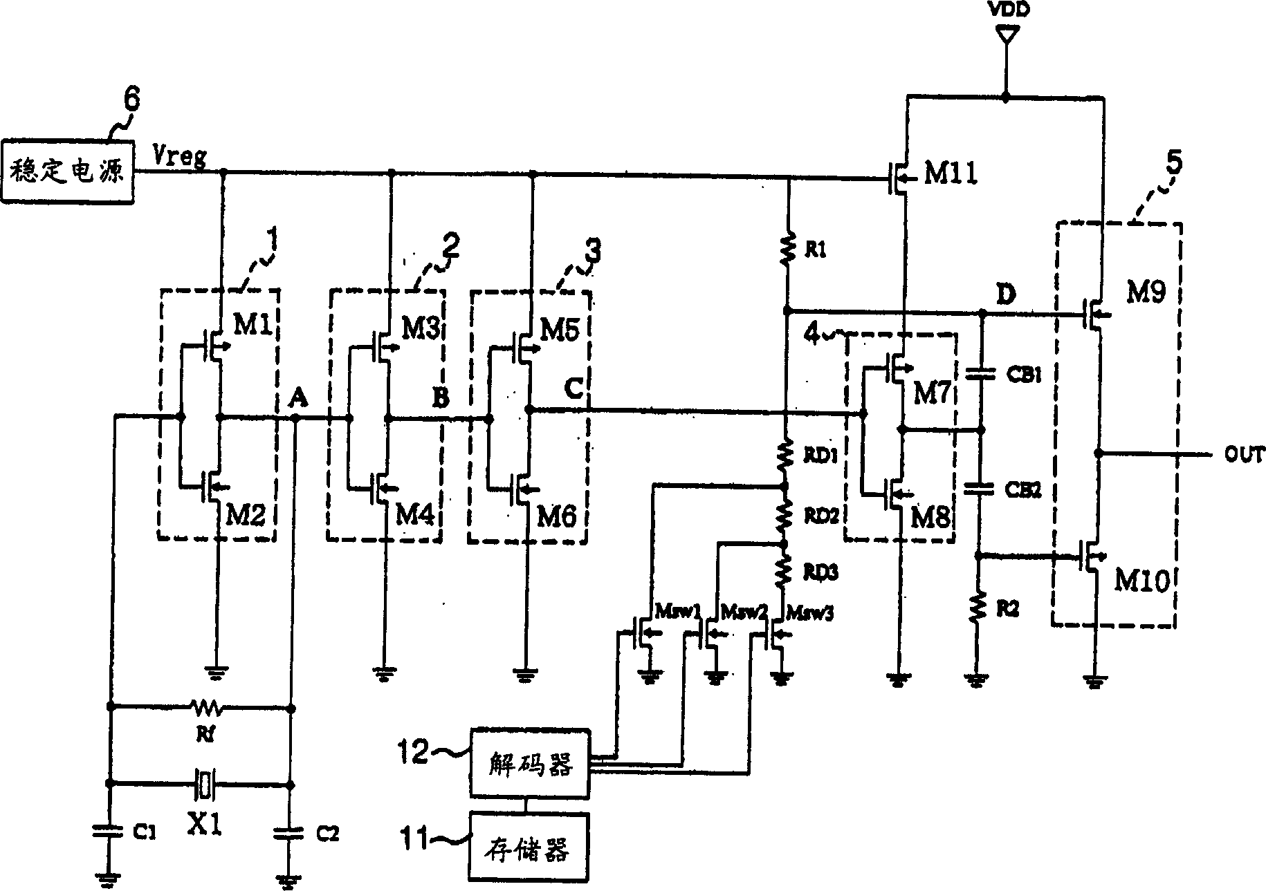
[0033] figure 1 It is a circuit diagram showing an embodiment of a crystal oscillation circuit as a piezoelectric oscillation circuit of the present invention.

[0034] In addition, parts having the same functions as those of the crystal oscillation circuit shown in FIGS. 8 and 9 are given the same reference numerals, and detailed description thereof will be omitted.

[0035] in the figure 1 Among them, A is an output terminal of the oscillation amplifier circuit 1 , B is an output terminal of the first buffer circuit 2 , and C is an output terminal of the second buffer circuit 3 .

[0036] The gate of the depletion MOS transistor M11, the Pch-CMOS transistor M1 of the oscillation amplifier circuit 1, the Pch-CMOS transistor M3 of the first buffer circuit 2, and the second buffer circuit 3 are respectively connected to the output line of the stable power supply 6. The source of the Pch-CMOS transistor M5.

[0037] In addition, in this embodiment, an example was given in whi...


PUM


Abstract

Provides piezoelectric oscillation circuits that can obtain stable oscillation characteristics over a wide range of power supply voltages and can adjust the oscillation output amplitude. The circuit includes: a stabilized power supply (6) that stabilizes the voltage fluctuation of the DC voltage supplied from the DC power supply VDD; an oscillation circuit section (1) that uses a crystal vibrator (X1) as an oscillation source; ), using the output signal of the oscillating circuit part (1) as an input, connecting a multi-stage inverter circuit in series, and connecting a depletion-type MOS transistor on the last stage inverter circuit; the output amplification of the output of the amplifying buffer circuit (4) The circuit (5) is characterized in that it has: an output level adjustment circuit, which is composed of a plurality of MOS switches (Msw1~Msw3) and resistance elements (RD1~RD3), and can change the Nch-transistors constituting the output amplifier circuit (5). (M9) gate voltage to adjust the output level; storage circuit (11), storing data for selecting any one of a plurality of MOS switches; decoder (12), according to the data stored in the storage circuit (11) An analog signal input to the MOS switch is generated.

Description

technical field [0001] The invention relates to a piezoelectric oscillating circuit, which is especially suitable for a low-power consumption temperature-compensated crystal oscillator (TCXO) and the like. Background technique [0002] In recent years, there has been a strong demand for downsizing and weight reduction of portable devices used in mobile communications such as mobile phones, and quartz oscillator circuits used as frequency references for these portable devices have also been required to be downsized. [0003] FIG. 8 is a circuit diagram showing an example of a circuit configuration of a conventional crystal oscillation circuit. [0004] In this FIG. 8, X1 is a quartz vibrator, Rf is a high-frequency resistor, C1 and C2 are capacitors for oscillation, 1 is an oscillation amplifier circuit, 2 is a first snubber circuit (primary snubber circuit), and 3 is a second snubber circuit ( Second stage buffer circuit), 4 is the third buffer circuit (third stage buffer c...

Claims


Application Information

Patent Timeline
Patent Type & Authority Applications(China)
IPC IPC(8): H03B5/32H03B5/36
CPCH03B5/04H03B5/364H03B2200/0034H03B2200/0046H03B5/32
Inventor 山本壮洋
Owner TOYO TSUSHINKI
Why Eureka
Try Eureka