Phase-locked loop circuit comprising voltage-controlled oscillator having variable gain

a phase-locked loop and oscillator technology, applied in the direction of electrical apparatus, pulse automatic control, etc., can solve the problems of reducing q-value, vco may exhibit nonlinear characteristics, and further limit the tuning range of pll circuits, so as to improve phase noise characteristics and wide operating frequency

Inactive Publication Date: 2012-09-25
ELECTRONICS & TELECOMM RES INST
View PDF13 Cites 5 Cited by
  • Summary
  • Abstract
  • Description
  • Claims
  • Application Information

AI Technical Summary

Benefits of technology

[0009]The present invention is directed to a phase-locked loop (PLL) circuit in which a voltage-controlled oscillator (VCO) has different gains according to a mode transition so that the PLL circuit may ensure a wide operating frequency and an improved phase noise characteristic.
[0010]Also, the present invention is directed to a PLL circuit configured to increase a tuning range without increasing the number of capacitor banks to reduce a designed area and improve the performance of the entire circuit.

Problems solved by technology

That is, as the power supply voltage of the PLL circuit decreases, a tuning range of the PLL circuit may be further limited.
However, when the number of the capacitor banks is increased, the entire designed area may be increased, and a VCO may exhibit a nonlinear characteristic according to the number of capacitor banks.
Also, when a large number of capacitor banks are provided, a parasitic capacitor and a leakage current may be caused to the output of the VCO, thereby reducing a Q-value.
Meanwhile, when the number of inductors is increased, the designed area may be limited, and the use of the VCO with a large gain may worsen noise characteristics of the PLL circuit.
That is, when the VCO has a great gain, the frequency of the VCO may be greatly varied due to noises of the control voltage of the PLL circuit, thereby adversely affecting the noise characteristics of the PLL circuit.

Method used


Image

  • Phase-locked loop circuit comprising voltage-controlled oscillator having variable gain
  • Phase-locked loop circuit comprising voltage-controlled oscillator having variable gain
  • Phase-locked loop circuit comprising voltage-controlled oscillator having variable gain

Examples


embodiment

Configuration of a Phase-locked Loop (PLL) Circuit

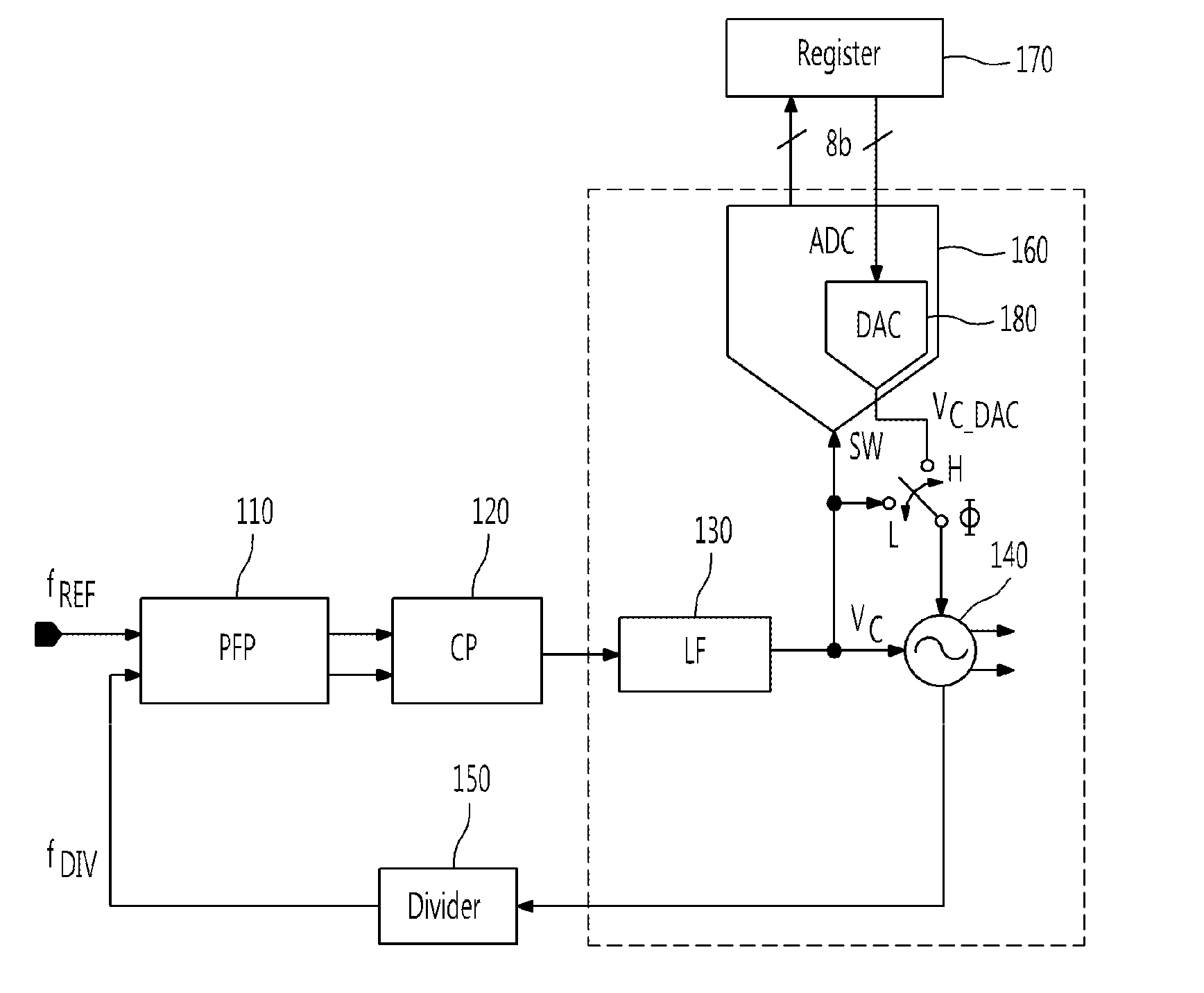
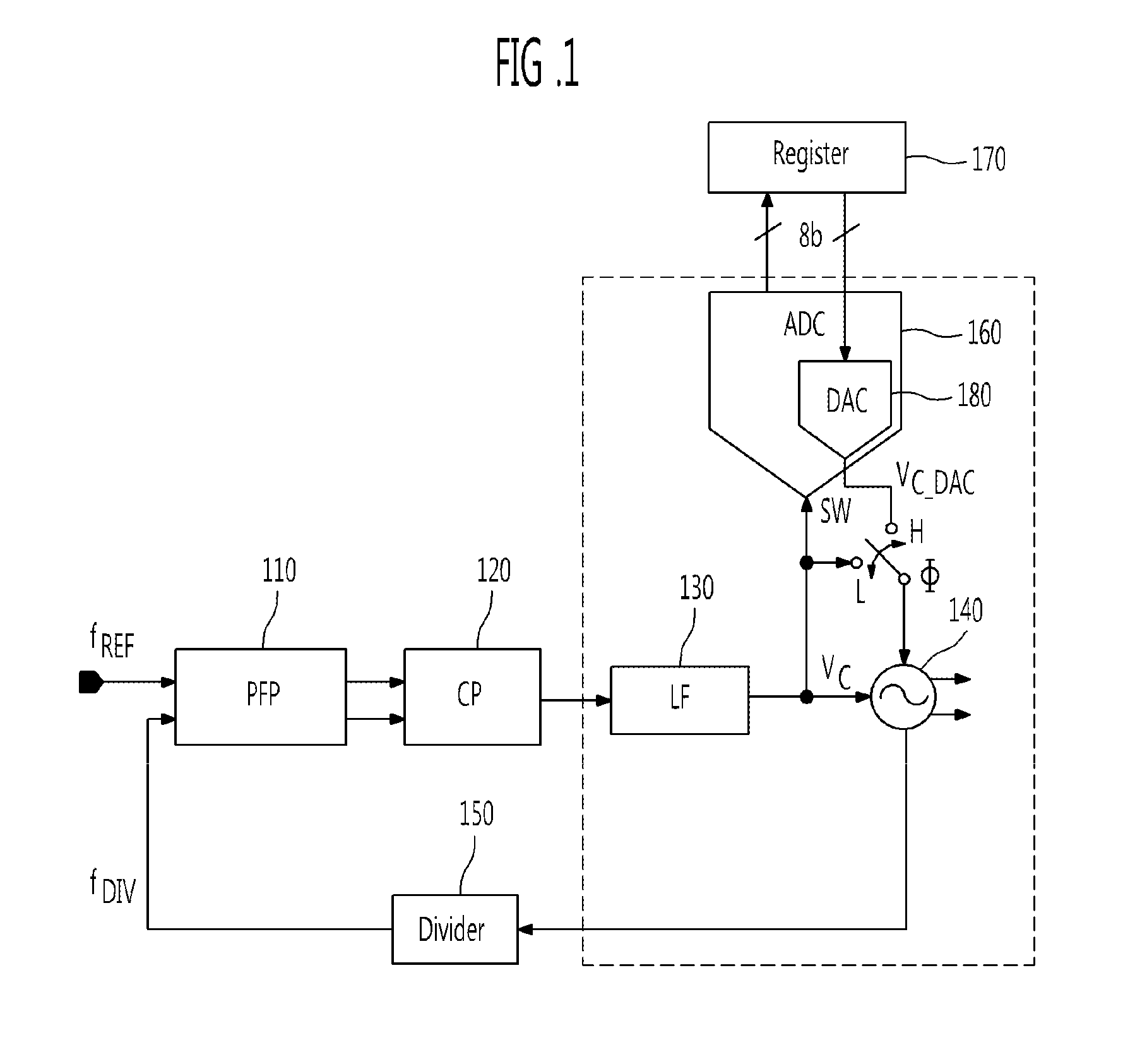
[0027]FIG. 1 is a block diagram of the entire configuration of a PLL circuit according to an exemplary embodiment of the present invention.

[0028]Referring to FIG. 1, a PLL circuit according to the present invention may have a basic loop including a phase frequency detector (PFD) 110, a charge pump (CP) 120, a loop filter (LF) 130, a voltage-controlled oscillator (VCO) 140, and a divider 150.

[0029]Also, the PLL circuit may further include an analog-to-digital converter (ADC) 160, a register 170, and a digital-to-analog converter (DAC) 180. The ADC 160 may receive an output voltage VC of the loop filter 130. The register 170 may store a digital code, which is an output value of the ADC 160. The DAC 180 may receive the digital code stored in the register 170.

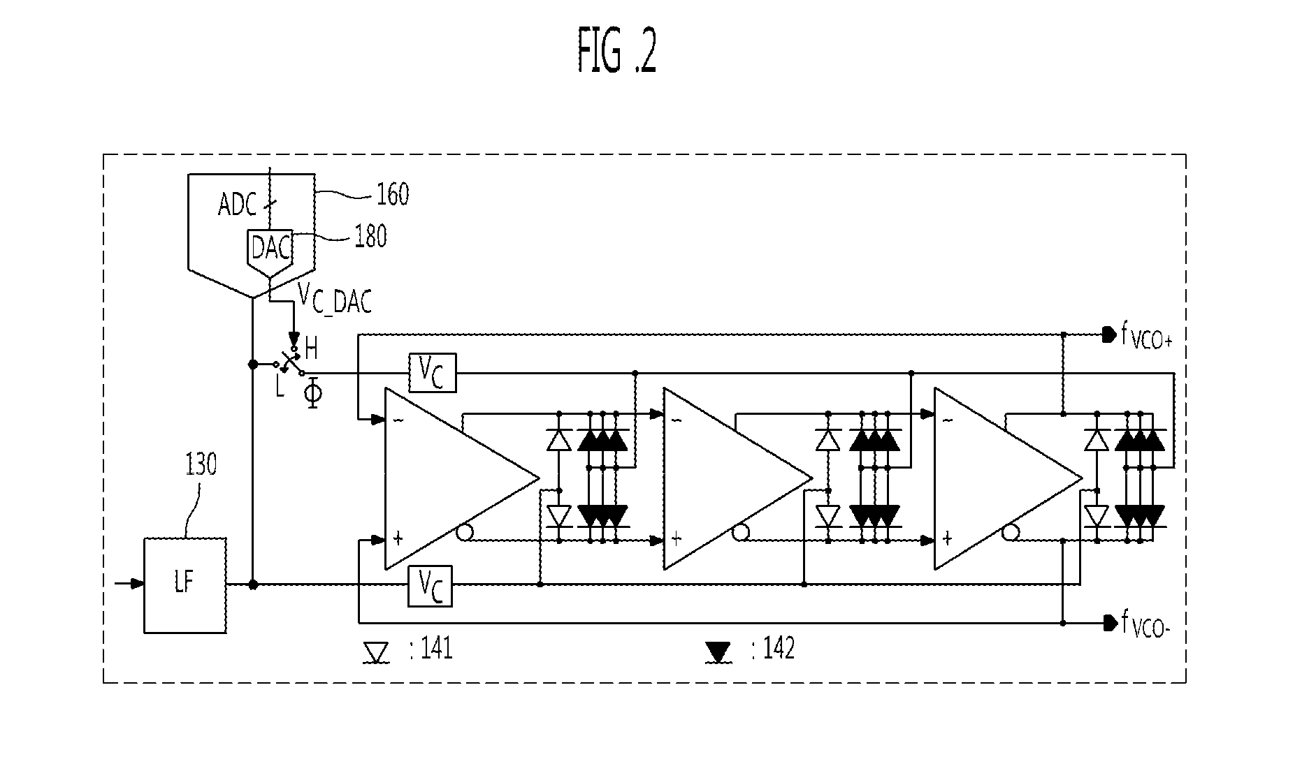
[0030]Meanwhile, the PLL circuit may further include a switch SW, which may allow one of the output signal VC of the loop filter 130 and an output signal VC—DAC of the DAC 180 to be...


PUM


Abstract

A phase-locked loop (PLL) circuit including a voltage-controlled oscillator (VCO) with a variable gain is provided. A phase frequency detector (PFD) detects a phase difference between a reference signal and a PLL feedback signal. A charge pump and a loop filter sequentially process an output signal of the PFD. A VCO has different gains according to a mode transition. A control voltage applied to the VCO is selected from an output signal of the loop filter and an additional control signal according to the mode transition.

Description

CROSS-REFERENCE TO RELATED APPLICATION[0001]This application claims priority to and the benefit of Korean Patent Application No. 10-2009-0128042, filed Dec. 21, 2009, and Korean Patent Application No. 10-2010-0032656, filed Apr. 9, 2010, the disclosure of which is incorporated herein by reference in its entirety.BACKGROUND[0002]1. Field of the Invention[0003]The present invention relates to a phase-locked loop (PLL) circuit including a voltage-controlled oscillator (VCO) having a variable gain and, more particularly, to a PLL circuit in which a VCO has different gains according to a mode transition to ensure a wide operating frequency and improve a phase noise characteristic.[0004]2. Discussion of Related Art[0005]In general, a phase-locked loop (PLL) circuit is a frequency feedback circuit configured to generate a signal having an arbitrary frequency in response to the frequency of an externally applied signal. The PLL circuit may detect a phase difference between a reference signa...

Claims


Application Information

Patent Timeline
Patent Type & Authority Patents(United States)
IPC IPC(8): H03L7/06
CPCH03L7/099H03L7/0995H03L2207/06
Inventor CHO, SANG HYUNLEE, HUI DONGKIM, KWI DONGKWON, JONG KEERYU, SEUNG TAK
Owner ELECTRONICS & TELECOMM RES INST
Why Eureka
Try Eureka