Printing device and use method thereof

A printing device and printing board technology, applied in the direction of conductive pattern formation and other directions

Active Publication Date: 2006-11-15
ORIENT SEMICON ELECTRONICS
View PDF0 Cites 8 Cited by
  • Summary
  • Abstract
  • Description
  • Claims
  • Application Information

AI Technical Summary

Problems solved by technology

[0005] The main purpose of the present invention is to provide a printing device and its use method to solve the problems in the prior art

Method used


Image

  • Printing device and use method thereof
  • Printing device and use method thereof
  • Printing device and use method thereof

Examples


Embodiment Construction

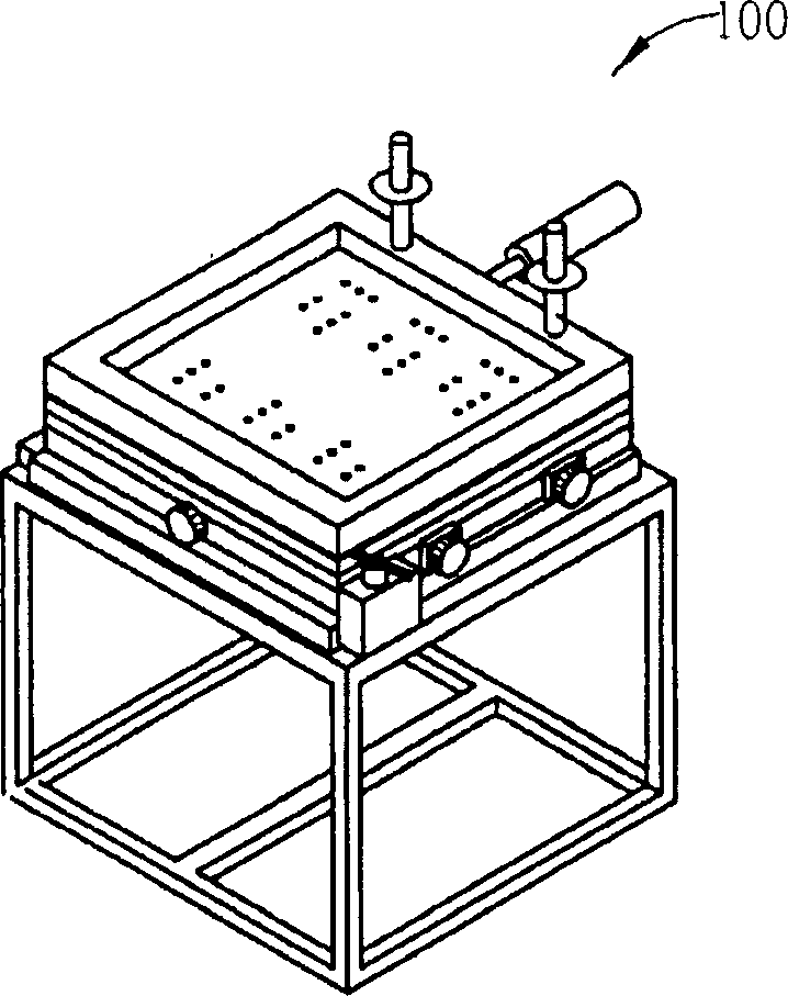
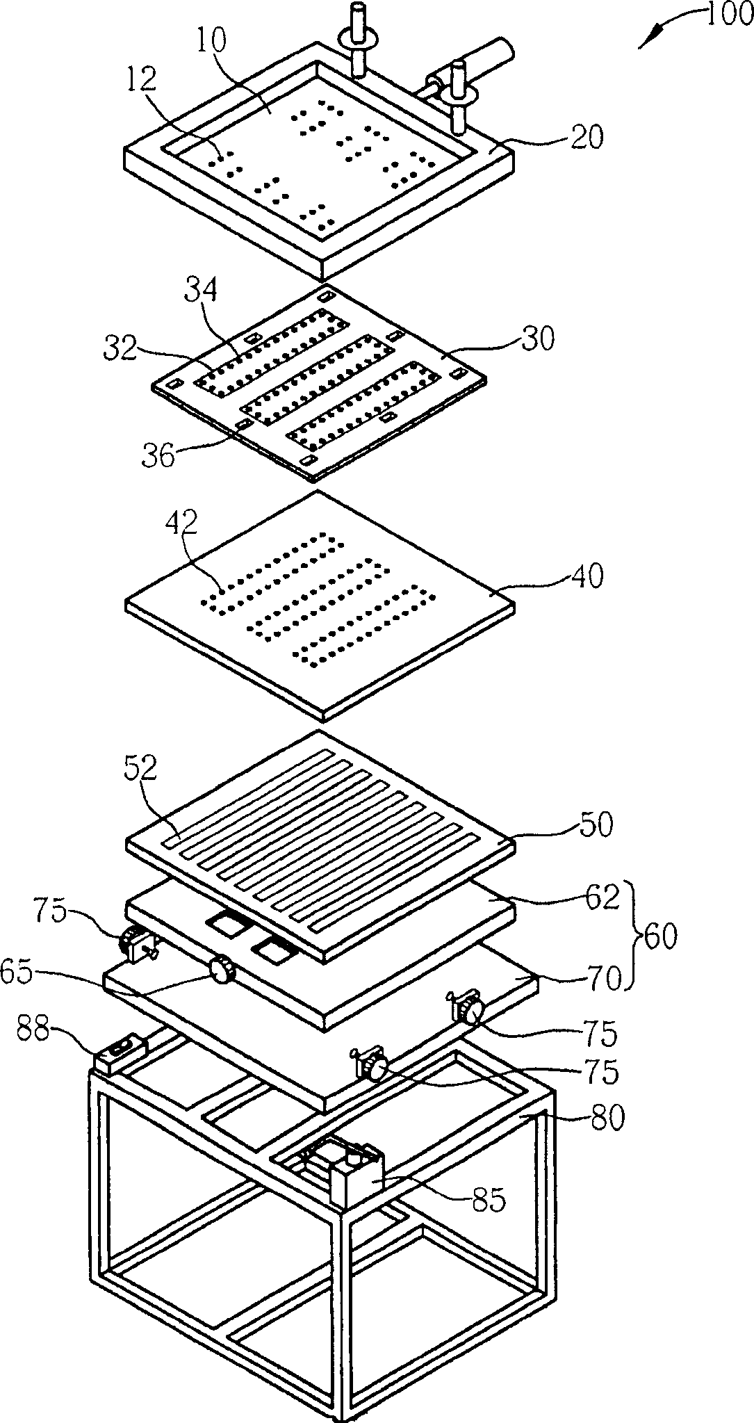
[0028] Please refer to figure 1 and figure 2 , figure 1 It is a schematic structural diagram of a printing device 100 in a preferred embodiment of the present invention, figure 2 It is an exploded schematic view of each component of the structure of the printing device 100 according to the preferred embodiment of the present invention. Such as figure 2 As shown, the structure of the printing device 100 of the present invention includes a printing plate 10 , a printing plate supporting and fixing module 20 , a loading plate 30 , an upper template 40 , a lower template 50 , a fine-tuning module 60 and a support frame 80 .

[0029] The surface of the printing plate 10 includes at least one printing opening 12 . The printing openings 12 can be set correspondingly according to the positions of the pads on the surface of the circuit board (not shown) where the solder paste is to be printed, so that during the printing process, the solder paste can be printed onto the circuit ...


PUM


Abstract

This invention discloses a printing device including a PB, a load board and a vacuum module, in which, at least one open-end is set on the surface of the PB, the loading board is under the PB and set with a locating groove and multiple first holes on the surface, besides, the vacuum module is under the loading board and adsorbs the upper part of the loading board by the first holes, the printing device also includes a top cover board and utilizes multiple fixing clamps to fasten the top cover board and the loading board.

Description

technical field [0001] The present invention relates to a printing device (printer) and its usage method, in particular to a printing device which can be used for printing long-sized circuit boards and its usage method. Background technique [0002] Generally speaking, circuit boards are roughly divided into rigid circuit boards and flexible circuit boards. The early flexible circuit boards were mainly used in the fields of small or thin electronic mechanisms and connections between hard circuit boards. In the late 1970s, they were gradually used in electronic information products such as computers, cameras, printers, car audio and hard drives. [0003] In the prior art, before placing chips, resistors, capacitors and other parts on the flexible circuit board by using the placement machine, it is usually necessary to apply a layer of solder paste on the position of the flexible circuit board through the printing machine. However, the maximum size of the flexible circuit boa...

Claims


Application Information

Patent Timeline
IPC IPC(8): H05K3/12
Inventor 李升学高宏宜
Owner ORIENT SEMICON ELECTRONICS
Why Eureka
Try Eureka