Methods and devices for fabricating three-dimensional nanoscale structures

一种纳米、辐射敏感材料的技术,应用在用于制造三维纳米级结构和装置领域,能够解决形成图案大量结构困难、劳动强度大、几何形状、物理尺度和尺寸限制等问题

Active Publication Date: 2007-01-03
THE BOARD OF TRUSTEES OF THE UNIV OF ILLINOIS
View PDF0 Cites 18 Cited by
  • Summary
  • Abstract
  • Description
  • Claims
  • Application Information

AI Technical Summary

Problems solved by technology

However, these techniques have certain limitations in the geometry, physical scale and size of the patterns it can produce
For example, two-photon lithography is capable of producing a wide variety of structures, but its serial operation makes patterning large substrate areas or generating large numbers of structures difficult and labor-intensive

Method used


Image

  • Methods and devices for fabricating three-dimensional nanoscale structures
  • Methods and devices for fabricating three-dimensional nanoscale structures
  • Methods and devices for fabricating three-dimensional nanoscale structures

Examples


Embodiment 1

[0109] Example 1: Fabrication of Porous Nanofilters Integrated in Microfluidic Channels

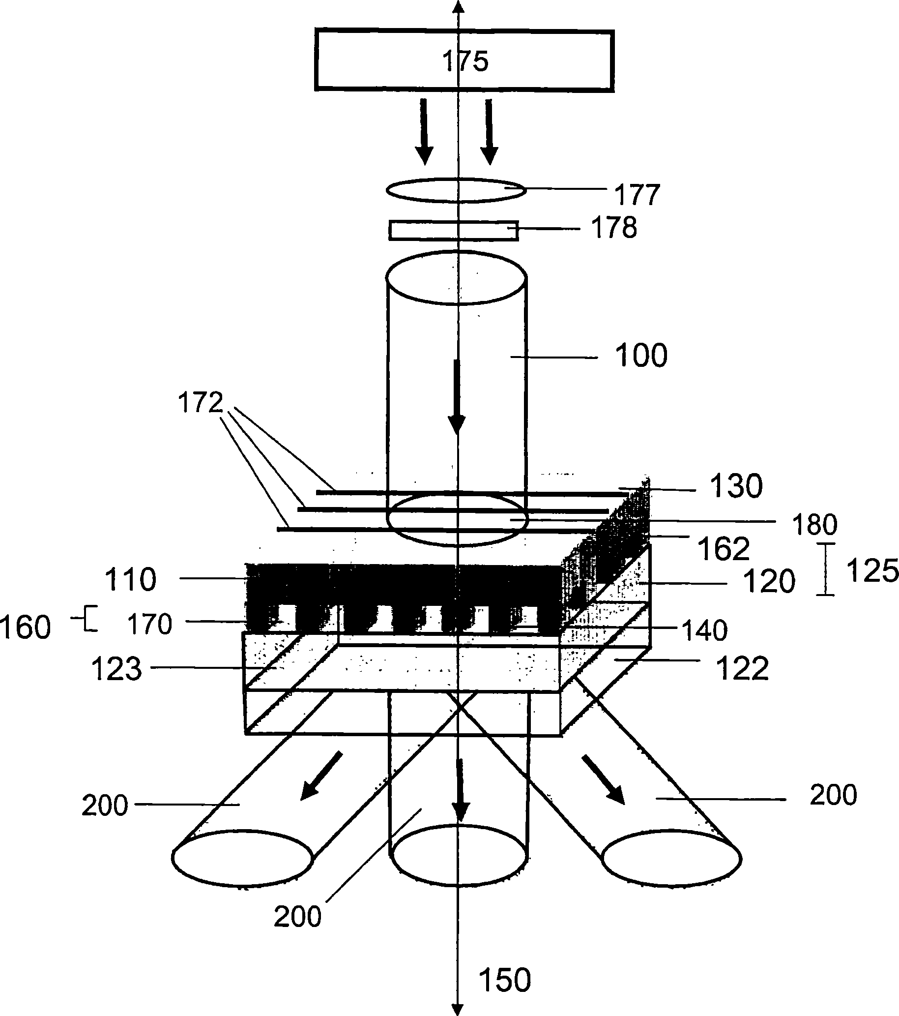
[0110] The practical application of 3D nanostructures relies heavily on their mechanical strength and their ability to be integrated into microsystems, nanosystems, and / or large-scale assemblies to form functional devices. To evaluate the utility of nanostructures produced by the methods and devices of the present invention, porous nanofilters were fabricated and integrated into microfluidic channels of a microfluidic system. The ability of the method and device of the present invention to fabricate useful 3D structures is demonstrated by the excellent mechanical and filtration properties exhibited by the constructed nanoporous filters.

[0111] To exemplify these properties, 3D nanostructured filter elements containing multiple 3D nanostructures were fabricated and integrated into channels of a microfluidic system for the separation of submicron particles from fluids. A suitable phase m...

Embodiment 2

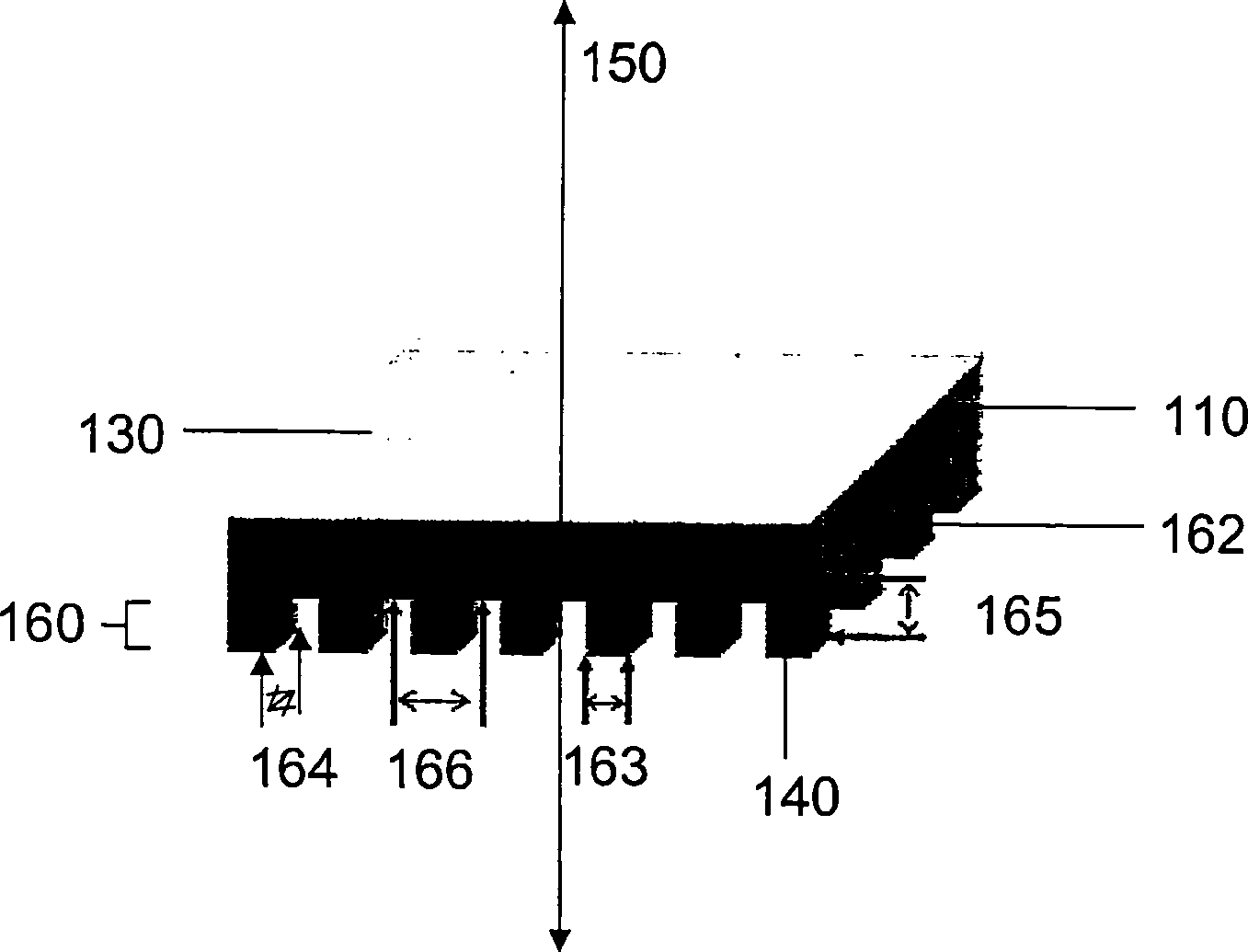
[0116] Example 2: Model calculations of the intensity distribution and nanostructures produced by the phase mask of the present invention

[0117] Figure 7A-L Scanning electron micrographs and simulation results of various periodic structures that can be fabricated on a large scale using the method of the present invention are presented (see inset). These methods are versatile and can be used with a variety of phase mask types, optical configurations, and light sources, such as visible and ultraviolet lasers, and filtered mercury lamps. Rigorous coupled wave analysis defines various Calculated intensity distribution of the situation. Quantitative analysis of the simulation results and scanning electron micrographs show a good agreement between the calculated intensity distribution and the shape of the 3D nanostructures produced using the method of the present invention.

[0118] The simulations employ rigorous coupled wave analysis (RCWA) combined with concepts from Abbe's...

Embodiment 3

[0126] Example 3: Selective Variation of Spatial and Temporal Coherence of Electromagnetic Radiation Used by the Method of the Invention

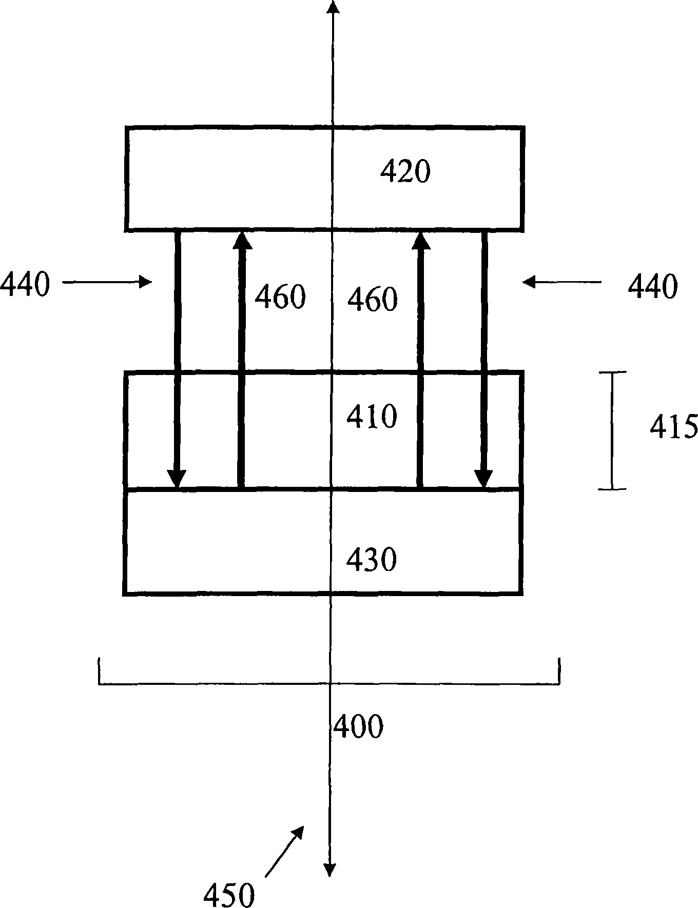
[0127] In an embodiment of the invention useful in a variety of fabrication applications, the spatial coherence and / or temporal coherence of the electromagnetic radiation employed by the method of the invention is selectively tuned to control important structural features of the fabricated 3D structures, For example 3D structured regions where nanoscale and / or microscale components are located. In the methods of the present invention, selected structural features are optimized for a variety of applications, device configurations and device environments using the control provided by selective changes in spatial and / or temporal coherence.

[0128] In one embodiment, the temporal coherence and / or spatial coherence of electromagnetic radiation directed at a mask element in optical communication with the radiation-sensitive material is selected ...


PUM

PropertyMeasurementUnit
wavelengthaaaaaaaaaa
diameteraaaaaaaaaa
sizeaaaaaaaaaa

Abstract

The present invention provides methods and devices for fabricating 3D structures and patterns of 3D structures on substrate surfaces, including symmetrical and asymmetrical patterns of 3D structures. Methods of the present invention provide a means of fabricating 3D structures having accurately selected physical dimensions, including lateral and vertical dimensions ranging from 10s of nanometers to 1000s of nanometers. In one aspect, methods are provided using a mask element comprising a conformable, elastomeric phase mask capable of establishing conformal contact with a radiation sensitive material undergoing photoprocessing. In another aspect, the temporal and / or spatial coherence of electromagnetic radiation using for photoprocessing is selected to fabricate complex structures having nanoscale features that do not extend entirely through the thickness of the structure fabricated.

Description

[0001] Cross References to Related Applications [0002] This application claims priority under 35 U.S.C. 119(e) to U.S. Provisional Patent Applications 60 / 526,245 and 60 / 598,404, filed December 1, 2003, and August 2, 2004, respectively, which are incorporated herein by reference The entire content thereof is incorporated into this specification without contradicting the content disclosed in the present application. Background technique [0003] Advances in nanoscience and technology increasingly rely on techniques for fabricating structures that include features with selected nanoscale physical dimensions, such as length, height, and width. Emerging methods in the microelectronics industry, such as deep UV projection mode lithography and electron beam lithography, are well suited for patterning two-dimensional (2D) nanostructures on ultraflat glass or semiconductor surfaces. However, the limited depth of focus of these methods makes the direct fabrication of the types of thr...

Claims


Application Information

Patent Timeline
Patent Type & Authority Applications(China)
IPC IPC(8): G03F7/00G03F7/20B81C99/00B82BB82B3/00G03F1/00G03F1/60
CPCB82Y10/00B82B3/00G03F7/7035G03F7/703G03F1/60G03F1/14Y10S430/146G03F7/70408B82Y40/00B82Y30/00G03F7/70283G03F1/50G03F7/00G03F7/20G03F7/26B81C99/00
Inventor J·A·罗杰斯S·全J·朴
Owner THE BOARD OF TRUSTEES OF THE UNIV OF ILLINOIS
Why Eureka
Try Eureka