Method and circuit for processing chip reset

A technology for processing chips and circuits, which is applied in the field of processing chip resets. It can solve the problems of reset signal position deviation, uncertain initial state of registers, increased circuit design complexity, power consumption, and chip area, so as to ensure stability and simplify wiring. , the effect of small area

Inactive Publication Date: 2007-03-21
CHIPHOMER TECH SHANGHAI
View PDF0 Cites 14 Cited by
  • Summary
  • Abstract
  • Description
  • Claims
  • Application Information

AI Technical Summary

Problems solved by technology

However, using the prior reset circuit, the asynchronous reset signal is directly connected to the asynchronous clearing terminal of the register (composed of several trigger units), and the exit reset state is asynchronous, thus causing the initial state of each register to be uncertain, and even causing the chip to reset. Can not work normally
As shown in Figure 2, the timing diagram of the reset signal connected to the two flip-flops A and B in Figure 1 and the timing diagram of the output of the Q terminal, as shown in the figure, the delay between the reset signal and the asynchronous reset terminal R of the flip-flop A and The delay to the asynchronous reset terminal R of register B is inconsistent. If the delay difference is relatively large, it will cause a deviation in the position of the reset signal relative to the clock signal: one reset signal arrives before the rising edge of the clock, while the other After a reset signal arrives at the rising edge of the clock, it is likely to cause the initial state of the chip to be unstable, and it cannot be guaranteed that all registers in the same clock domain will exit the reset state within the same period, and the change edge of the reset signal is relative to the active edge of the clock. have a large enough distance
[0007] In the prior art, there are also attempts to solve the problem that the reset state cannot be jumped out at the same time, such as adding a delay buffer to compensate for the delay of the reset signal. More hardware units increase the complexity of circuit design, power consumption and chip area

Method used


Image

  • Method and circuit for processing chip reset
  • Method and circuit for processing chip reset
  • Method and circuit for processing chip reset

Examples


Embodiment Construction

[0037] The method and circuit for chip reset of the present invention will be described in detail below with reference to the drawings and embodiments.

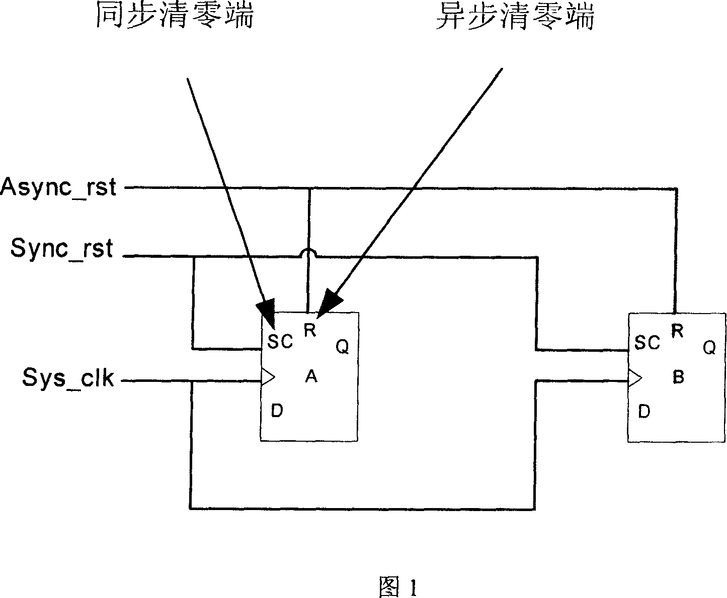
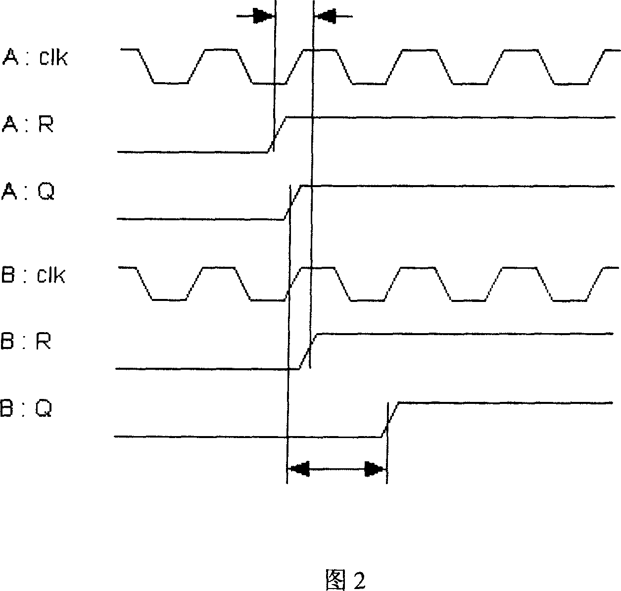
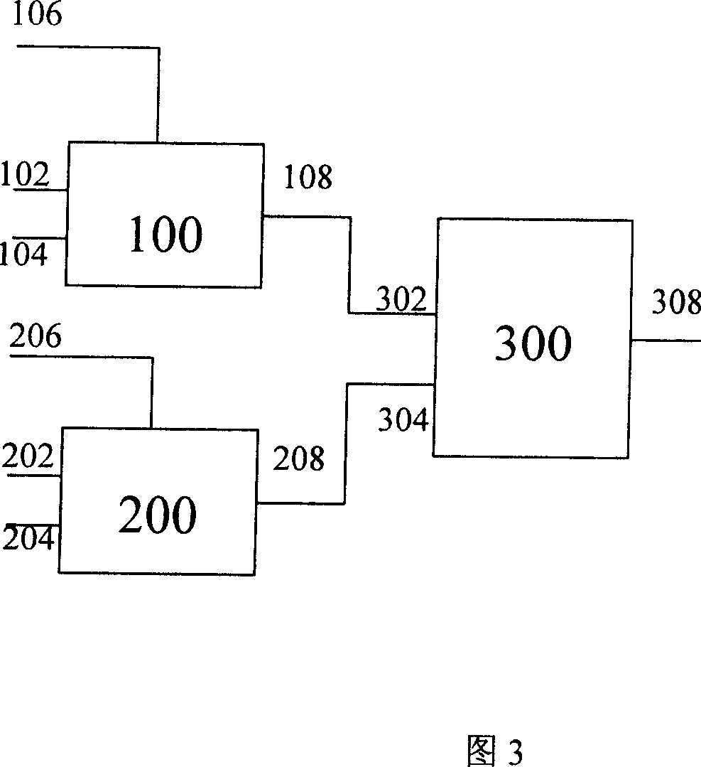
[0038] As shown in Figure 3 is a block diagram of the reset circuit of the present invention, as shown in the figure, the circuit includes: a first trigger unit 100 for triggering an asynchronous reset signal, including a clock port 102, a digital input port 104, an asynchronous reset port 106 and output port 108; The second trigger unit 200 for triggering a synchronous reset signal includes clock port 202, digital input port 204, asynchronous reset port 206 and output port 208; a combinational logic unit 300 includes several input ports 302, 304 and an output port 306; wherein: the output port 108 of the first trigger unit 100 is connected to the asynchronous reset port 206 of the second trigger unit 200, and the output port 108 of the first trigger unit 100 The output port 208 of the second trigger unit 200 is connected wit...


PUM


Abstract

The invention discloses a circuit used for slug resetting. It consists of two triggering units which are used to trigger asynchronous resetting signal and synchronous resetting signal and a logical combination unit. The output port of the one triggering unit was connected to the asynchronous resetting port of the other one. The output ports of the two triggering units were connected to the input port of the logical combination unit. The resetting signals were combined and connected to the asynchronous end of all triggers in the system clock. Asynchronous resetting and synchronous resetting were realized by this invention.

Description

technical field [0001] The invention relates to microelectronic design, in particular to a method and circuit for processing chip reset in digital integrated circuit design. Background technique [0002] In a digital integrated circuit chip, in order to ensure the normal operation of the chip, the reset circuit is an indispensable part. As the scale of the chip continues to increase, the structure of the reset circuit and its connection with other circuits become more and more complex. Especially in very large-scale integrated circuit chips, there are generally multiple clock domains, and each clock domain has its own synchronous reset signal; in addition, the chip also provides an asynchronous reset port to play the role of global reset. Since the reset circuit is crucial to the normal operation of the entire chip, its implementation must be simple in structure and high in reliability. [0003] The existing chip reset technology is generally to connect the asynchronous re...

Claims


Application Information

Patent Timeline
Patent Type & Authority Applications(China)
IPC IPC(8): G06F1/24
Inventor 陈军霞姚炜廖水清
Owner CHIPHOMER TECH SHANGHAI
Why Eureka
Try Eureka