Double-layer wideband rectangular microband paste antenna with non-radiant edged feeder
A microstrip patch antenna, non-radiative technology, applied in the structural form of radiating elements, antennas, electrical components, etc., can solve the problems of narrow bandwidth, shortening the length of feeding lines, etc., achieve large scanning angle, shortening feeding length, compression The effect of wiring space
- Summary
- Abstract
- Description
- Claims
- Application Information
AI Technical Summary
Problems solved by technology
Method used
Image

Examples
Embodiment 1
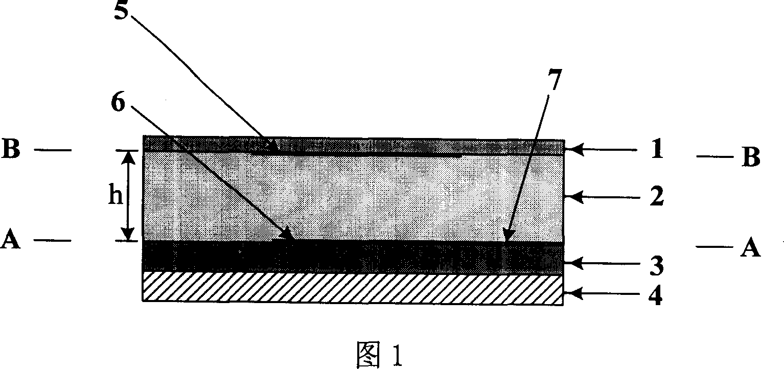
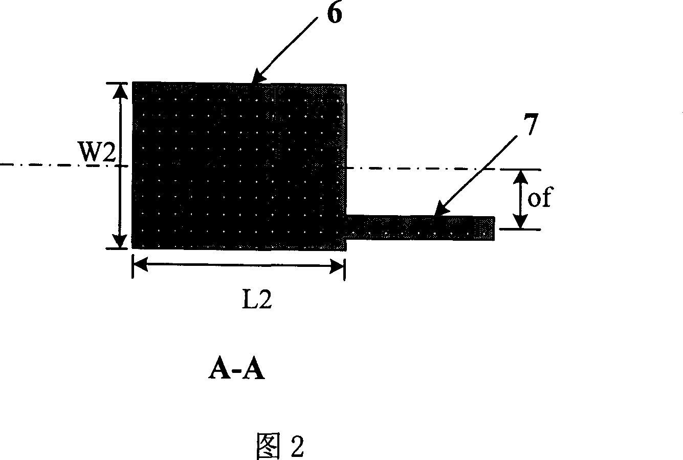
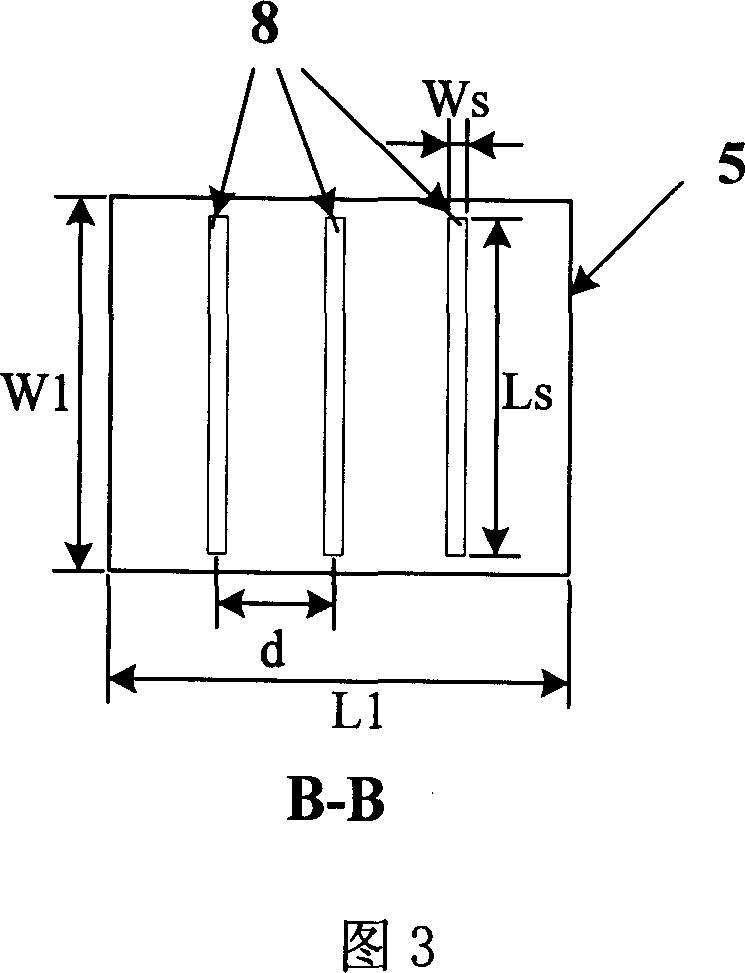
[0042] An X-band non-radiating edge-fed broadband double-layer microstrip patch antenna. The structure used in this antenna is exactly the same as that in FIG. 1 , and the microstrip line 7 is used for feeding, and three slots 8 are opened on the parasitic element 5 . Among them, the plate parameters of the parasitic dielectric plate 1 are: the thickness is 0.254mm, and the relative dielectric constant is 4.36; the foam plate with the relative dielectric constant of the intermediate dielectric layer 2 is 1.07, and the thickness h=0.093λ 0 ; The plate parameters of the feed medium plate 3 are: the thickness is 0.508, and the relative permittivity is 2.94. The geometric parameters of the parasitic element 5 are: the length of the radiation side L 1 =0.36λ 0 , the length ratio L of the radiating side to the non-radiating side 1 / W 1 =1.22; the geometric parameters of the feed element 6 are: the length L of the radiation side 2 =0.59λ 0 / ε r3 0.5 , the length ratio L of th...
Embodiment 2
[0052] An S-band non-radiating edge-fed broadband double-layer microstrip patch antenna. The structural form of the antenna is basically the same as that in FIG. 1 , and the microstrip line is used for feeding. The difference is that the parasitic element 5 is located above the parasitic dielectric plate 1 . There are six slits 8 on the parasitic element of the antenna, wherein the plate parameters of the parasitic dielectric plate 1 are: the thickness is 1.5 mm, and the relative dielectric constant is 2.55; the intermediate dielectric layer 2 is air with a relative dielectric constant of about 1.0, Thickness h=0.056λ 0 ; The plate parameters of the feed medium plate 3 are: the thickness is 1.5, and the relative permittivity is 2.55. The geometric parameters of the parasitic element 5 are: the length of the radiation side L 1 =0.32λ 0 , the length ratio L of the radiating side to the non-radiating side 1 / W 1 =1.1; the geometric parameters of the feed element 6 are: the l...
Embodiment 3
[0056] An L-band non-radiating edge-fed broadband double-layer microstrip patch antenna. The structure used in this antenna is basically the same as that in Figure 1, except that the coplanar feed of the microstrip line 7 is changed to a coaxial probe feed, and there are 3 slots on the parasitic element 5. Among them, the parameters of the parasitic dielectric board 1 are: the thickness is 1.524 mm, and the relative dielectric constant is 3.48; the intermediate dielectric layer 2 is a foam board with a relative dielectric constant of about 1.4, and the thickness h=0.045λ 0 ; The plate parameters of the feeding medium plate 3 are: the thickness is 2, and the relative permittivity is 4.5; the geometric parameters of the parasitic element 5 are: the length of the radiation side L 1 =0.35λ 0 , the length ratio L of the radiating side to the non-radiating side 1 / W 1 = 1.4; the geometric parameters of the feed element 6 are: the length L of the radiation side 2 =0.43λ 0 / ε r3...
PUM
| Property | Measurement | Unit |
|---|---|---|
| Thickness | aaaaa | aaaaa |
| Thickness | aaaaa | aaaaa |
| Thickness | aaaaa | aaaaa |
Abstract
Description
Claims
Application Information