Circuit board structure and making method

A circuit board and manufacturing method technology, which is applied in the direction of multilayer circuit manufacturing, including printed electrical components, and the formation of electrical connections of printed components, can solve the problems of increased process time, complicated process steps, and increased process costs, and achieve a reduction in process cost, shorten process time, and increase the effect of surface wiring density

Inactive Publication Date: 2007-06-13
PHOENIX PRECISION TECH CORP
View PDF0 Cites 10 Cited by
  • Summary
  • Abstract
  • Description
  • Claims
  • Application Information

AI Technical Summary

Problems solved by technology

[0008] Furthermore, in the above process, the circuit board with multiple circuit layers needs to prepare a core circuit board first, and then stack dielectric layers and circui

Method used


Image

  • Circuit board structure and making method
  • Circuit board structure and making method
  • Circuit board structure and making method

Examples


Embodiment

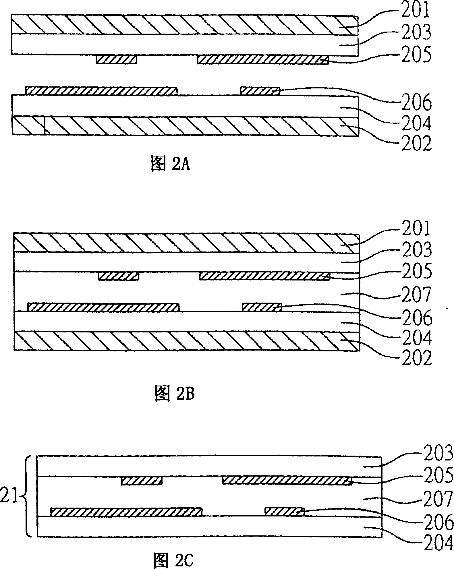
[0024] Please refer to FIGS. 2A to 2H , which are schematic cross-sectional views of the circuit board structure manufacturing method of the present invention.

[0025] Please refer to FIG. 2A , first a first carrier board 201 and a second carrier board 202 are provided, a first dielectric layer 203 is formed on the first carrier board 201, and a first dielectric layer 203 is formed on the first dielectric layer 203. Circuit layer 205 ; forming a second dielectric layer 204 on the second carrier board 202 , and forming a second circuit layer 206 on the second dielectric layer 204 . The above-mentioned first and second dielectric layers 203, 204 can be, for example, epoxy resin (Epoxy resin), polyimide (Polyimide), cyanate ester (Cyanate ester), glass fiber (Glass fiber), bisbutene Bismaleimide triazine (BT, Bismaleimide triazine) or mixed glass fiber and epoxy resin and other materials. The first dielectric layer 203 and the second dielectric layer 204 are made of the same ma...


PUM


Abstract

The invention provides a kind of circuit board's structure and its preparation method, which includes: to form No.1 and No. 2 dielectric layer on the No. 1 and No. 2 loading plate, then separate one side of the No. 1 and No. 2 circuit layer that are formed on the No. 1 and No. 2 loading plate into one No. 3 dielectric layer and then laminate them, embed the No. 1 circuit layer into the position between the No. 1 dielectric layer and the No. 3 dielectric layer, embed the No. 2 circuit layer into the position between the No. 2 dielectric layer and No. 3 dielectric layer, and to form a No. 3 circuit layer on the outer surface of the No. 1 dielectric layer, form a No. 4 circuit layer on the outer surface of the No. 2 dielectric layer; the circuit board structure of the invention includes: sandwich layer plate, No. 3 circuit layer, No. 4 circuit layer; the circuit board structure of the invention and its preparation method enhances the wiring density for the circuitry of the circuit board, shortens the path for transmitting signal, improves the electric property quality of the circuit board, simplies the working procedures, shortens the time for all working procedures and reduces the cost for all working procedures, lessens the thcickness of circuit board, which meets the development trendancy of micromation.

Description

technical field [0001] The present invention relates to a circuit board structure and its manufacturing method, in particular to a circuit board structure with multilayer circuits and its manufacturing method. Background technique [0002] With the vigorous development of the electronic industry, electronic products are gradually developing in the direction of lightness, thinness, shortness, smallness, high integration, multi-function, and high performance, and the integration of electronic components is also getting higher and higher. In order to meet the packaging requirements of high integration (Integration) and miniaturization (Miniaturization) of semiconductor packages, the circuit board (Circuit board) that provides multiple active and passive components and circuit connections has gradually evolved from a double-layer board structure to a multi-layer board ( Multi-layer board) structure, in a limited space, through the interlayer connection technology (Interlayer con...

Claims


Application Information

Patent Timeline
IPC IPC(8): H05K3/46H05K3/40H05K1/16
Inventor 王杏如王仙寿许诗滨
Owner PHOENIX PRECISION TECH CORP
Why Eureka
Try Eureka