Image sensor

a technology of image sensor and phase-dependent auto focusing, which is applied in the field of image sensor, can solve the problems of deteriorating af accuracy and image quality of dual pixel image sensor, and achieve the effect of increasing the accuracy of phase-dependent auto focusing and the image quality of the image sensor

Active Publication Date: 2018-07-03
SAMSUNG ELECTRONICS CO LTD
View PDF17 Cites 11 Cited by
  • Summary
  • Abstract
  • Description
  • Claims
  • Application Information

AI Technical Summary

Benefits of technology

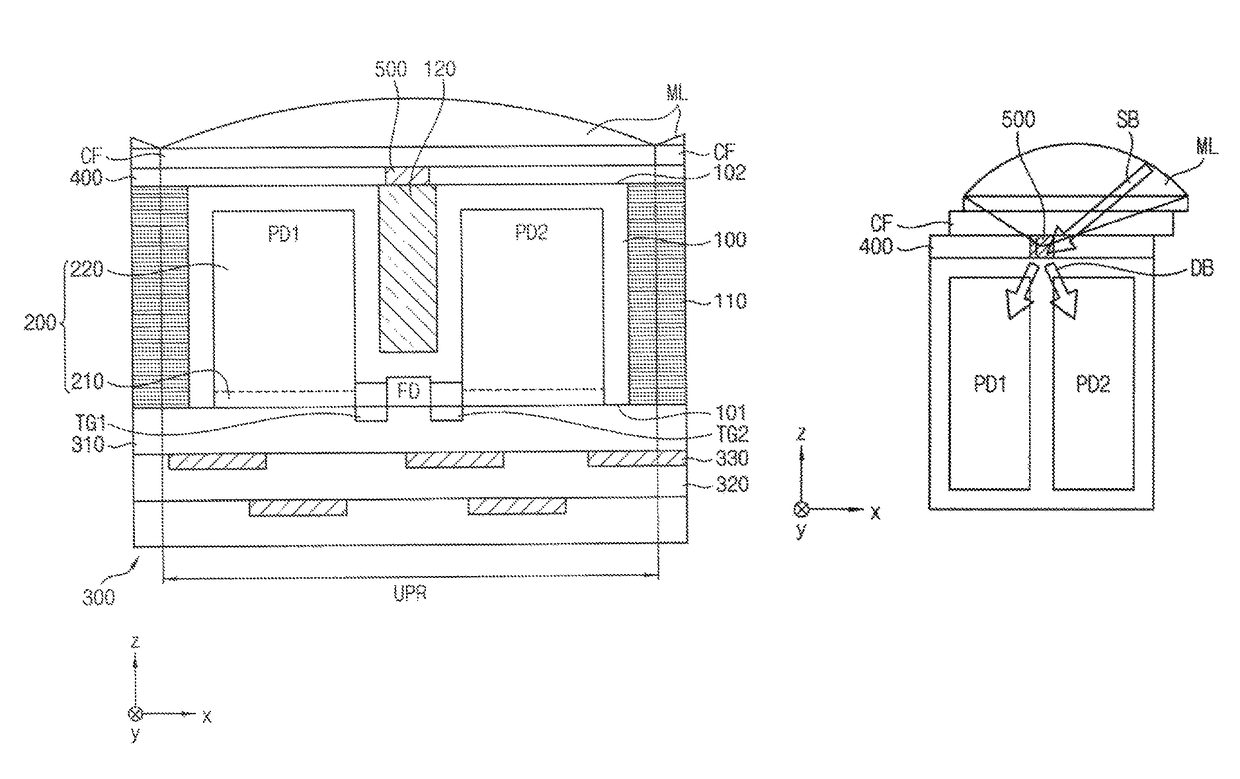
[0011]According to exemplary embodiments, the optical divider having the refractive index smaller than surroundings may be arranged on the boundary area of the photoelectrical converters and may be overlapped with the incident point at every unit pixel of the image sensor. Thus, the photoelectric converters may have substantially the same amount of light and the image signals generated from each of the photoelectric converters may have substantially the same intensity. As a result, the cross point of the image signals generated from each of the photoelectric converters may have similar phase irrespective of the wavelength of the slanted beam, so that the phase difference of each cross points of the image signals generated from the red, blue and green pixels are substantially negligible regardless of the wavelength of the slanted beam, thereby increasing the accuracy of the phase different auto focusing (PAF) and the image quality of the image sensor.

Problems solved by technology

However, since the penetration depth of a light beam is varied according to the wavelength thereof and the phase of the image signal may be varied by the penetration depth, the focus phases of each primary color light are also different in the dual pixel image sensor which generally deteriorate the AF accuracy and the image quality of the dual pixel image sensor.

Method used


Image

  • Image sensor
  • Image sensor
  • Image sensor

Examples


Embodiment Construction

[0030]Reference will now be made to the exemplary embodiments, which are illustrated in the accompanying drawings, wherein like reference numerals may refer to like components throughout.

[0031]The present disclosure now will be described more fully hereinafter with reference to the accompanying drawings, in which various exemplary embodiments are shown. The invention may, however, be embodied in many different forms and should not be construed as limited to the exemplary embodiments set forth herein. These example exemplary embodiments are just that—examples—and many embodiments and variations are possible that do not require the details provided herein. It should also be emphasized that the disclosure provides details of alternative examples, but such listing of alternatives is not exhaustive. Furthermore, any consistency of detail between various exemplary embodiments should not be interpreted as requiring such detail—it is impracticable to list every possible variation for every ...


PUM


Abstract

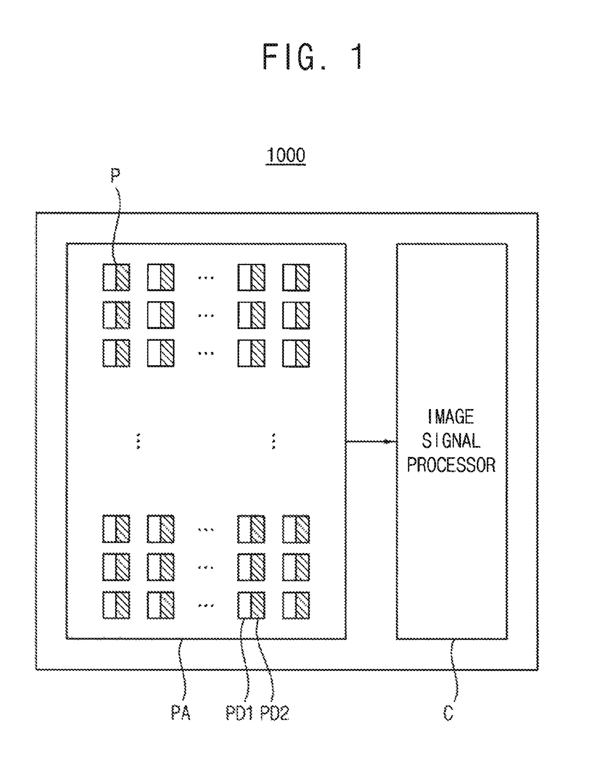
An image sensor includes multiple unit pixels defined by a pixel isolation layer on a substrate, at least a pair of photoelectric converters in each of the unit pixels and at least an optical divider on a rear surface of the substrate at each of the unit pixels. The photoelectric converters are separated by at least a converter separator in each of the unit pixels and generate photo electrons in response to an incident light that is incident to an incident point of the respective unit pixel. The optical divider is overlapped with the incident point and divides the incident light into a plurality of split lights having the same amount of light such that each of the photoelectric converters receives the same amount of light from the split lights.

Description

CROSS-REFERENCE TO RELATED APPLICATIONS[0001]This application claims priority under 35 U.S.C § 119 to Korean Patent Application No. 10-2016-0132006 filed on Oct. 12, 2016 in the Korean Intellectual Property Office, the contents of which are incorporated by reference herein in its entirety.BACKGROUND1. Field[0002]Example embodiments relate to an image sensor, and more particularly, to a CMOS image sensor having a plurality of photoelectric converters.2. Description of the Related Art[0003]Auto focusing (AF) technology has been widely adapted in recent image sensors. Particularly, phase difference auto focusing (PAF) technology has been intensively adapted in image sensors for realizing high focusing speed. According to PAF technology, a light passing through an imaging lens of an imaging device such as a camera is divided into split beams and the split beams are individually detected at different focus detection pixels as focus detection signals corresponding to respective focus dete...

Claims


Application Information

Patent Timeline
Patent Type & Authority Patents(United States)
IPC IPC(8): H01L27/146H04N5/232H04N5/225G02B7/36
CPCH01L27/14625H01L27/1463H01L27/14621H01L27/14645H04N5/2254H04N5/23212H01L27/14627G02B7/365H04N23/55H04N23/672H04N25/704H01L27/1464H01L27/14629
Inventor LEE, KYUNG-HO
Owner SAMSUNG ELECTRONICS CO LTD
Why Eureka
Try Eureka