

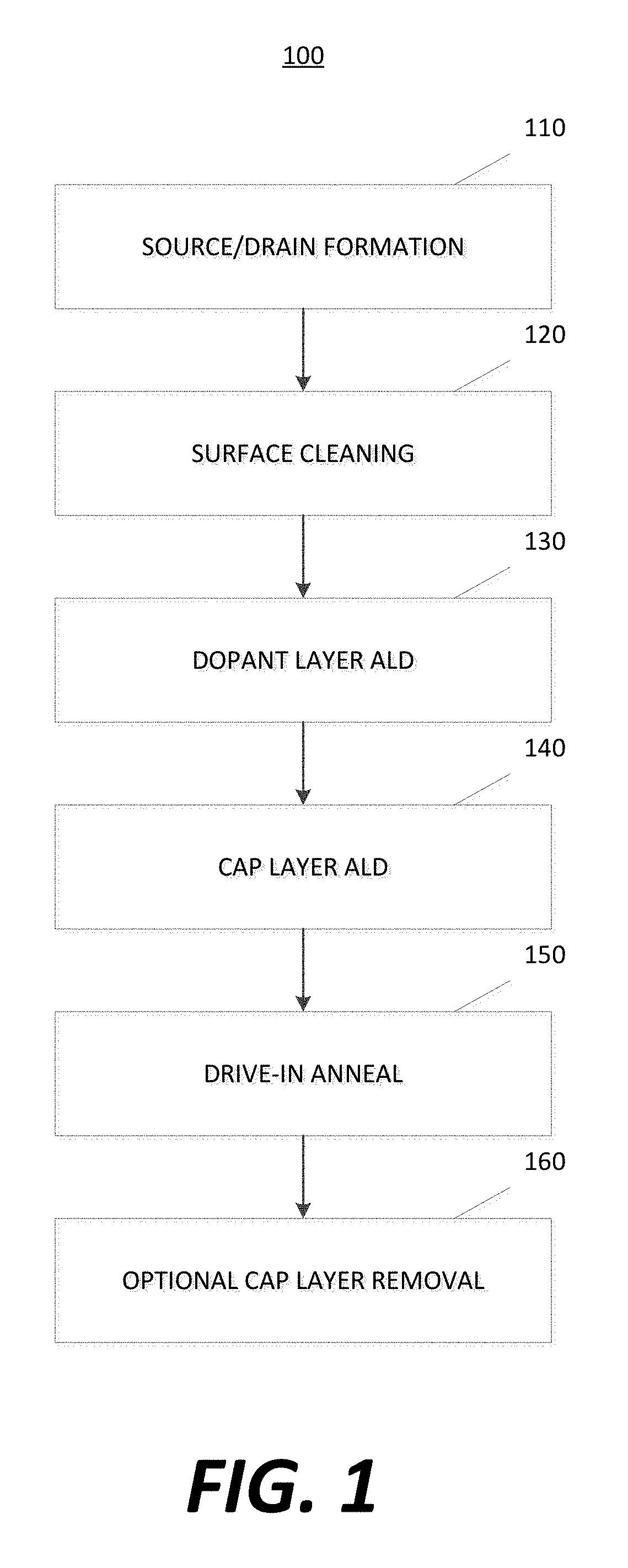
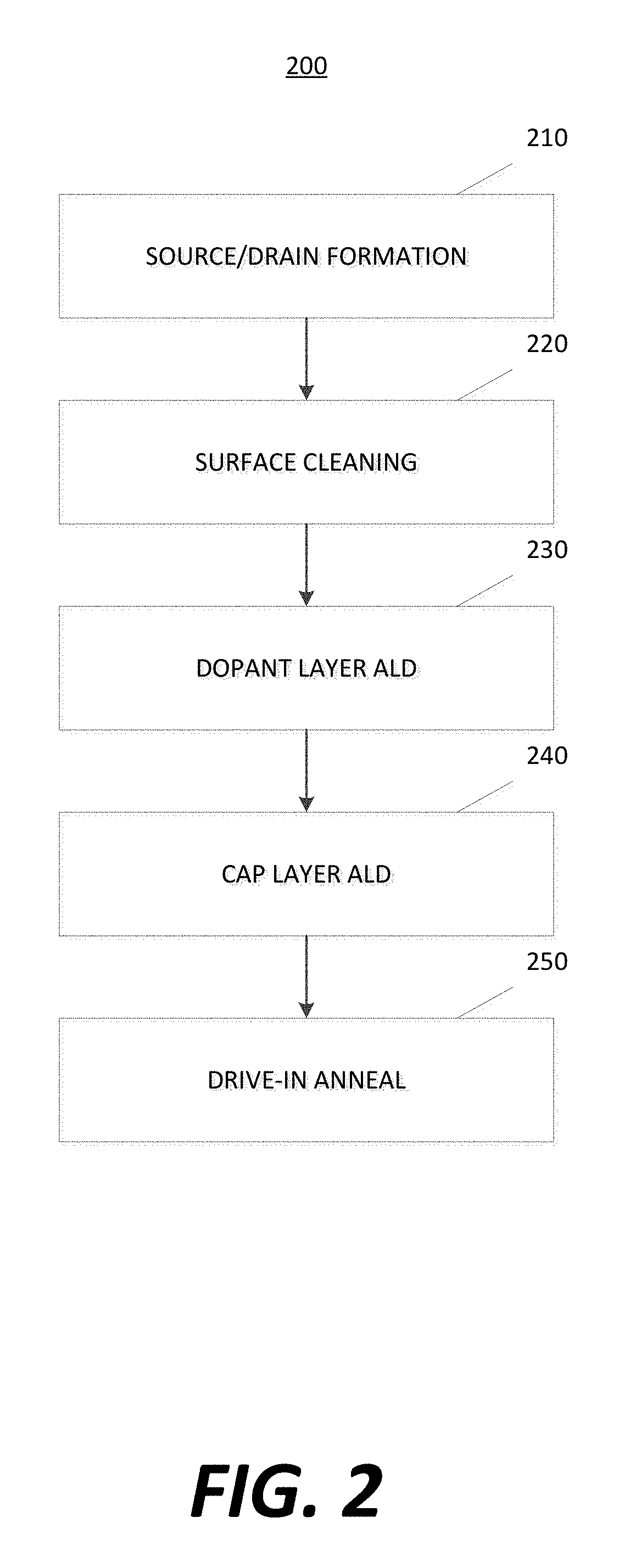
Source/drain performance through conformal solid state doping
a technology of solid state doping and source/drain, applied in the direction of semiconductor devices, electrical equipment, transistors, etc., can solve the problems of challenging the ion implantation process of finfet and nanowire devices
- Summary
- Abstract
- Description
- Claims
- Application Information
AI Technical Summary
Problems solved by technology
Method used
Image

Examples
Embodiment Construction
[0015]Although certain embodiments and examples are disclosed below, it will be understood by those in the art that the invention extends beyond the specifically disclosed embodiments and / or uses of the invention and obvious modifications and equivalents thereof. Thus, it is intended that the scope of the invention disclosed should not be limited by the particular disclosed embodiments described below.
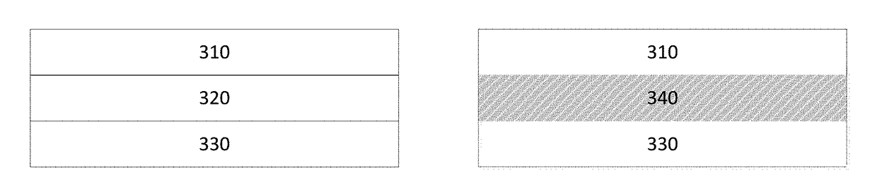
[0016]Atomic layer deposition (ALD) solid state doping (SSD) may be one way to form NMOS and CMOS devices. One reason for this may be the ability of ALD SSD to form films with excellent conformality and defect free features. Alternate doping methods, such as ion implantation, may introduce defects that ALD SSD can avoid during conformal doping of 3-D structures. ALD SSD also may provide the capability to deposit thin films with precise sub-nanometer thickness control, which thus determines the dose or number of atoms available at the surface to incorporate into the semiconductor as act...
PUM
 Abstract
Description
Claims
Application Information