Low Temperature Deposition of Silicon-Containing Films

a technology of low temperature deposition and silicon-containing films, which is applied in the direction of chemical vapor deposition coating, coating, plasma technique, etc., can solve the problems of increasing the complexity of the deposition process and the cost of the process

Active Publication Date: 2010-12-02
TOKYO ELECTRON LTD +1
View PDF31 Cites 442 Cited by
  • Summary
  • Abstract
  • Description
  • Claims
  • Application Information

AI Technical Summary

Benefits of technology

[0005]The current invention discloses the method of depositing silicon nitride, silicon oxynitride, silicon oxide, carbon-doped silicon nitride, carbon-doped silicon oxide and carbon-doped oxynitride films at low deposition temperatures. The silicon containing precursors used for the deposition are monochlorosilane (MCS) and monochloroalkylsilanes.

Problems solved by technology

But this may introduce unwanted impurity to the film, causing reliability issues for the devices that the film is suited for, and may also increase the complexity of the deposition process and cost.

Method used


Image

  • Low Temperature Deposition of Silicon-Containing Films
  • Low Temperature Deposition of Silicon-Containing Films

Examples


working example

Silicon Nitride Film

[0029]In this working example, a silicon oxide film has been deposited by using the following steps.

[0030]Substrates to be deposited films on were loaded to a hot wall atomic layer deposition (ALD) reactor. The reactor was flashed with Ar and pumped down to low pressure of less than 0.1 Torr (T) and heated up to a temperature at which film deposition was performed.

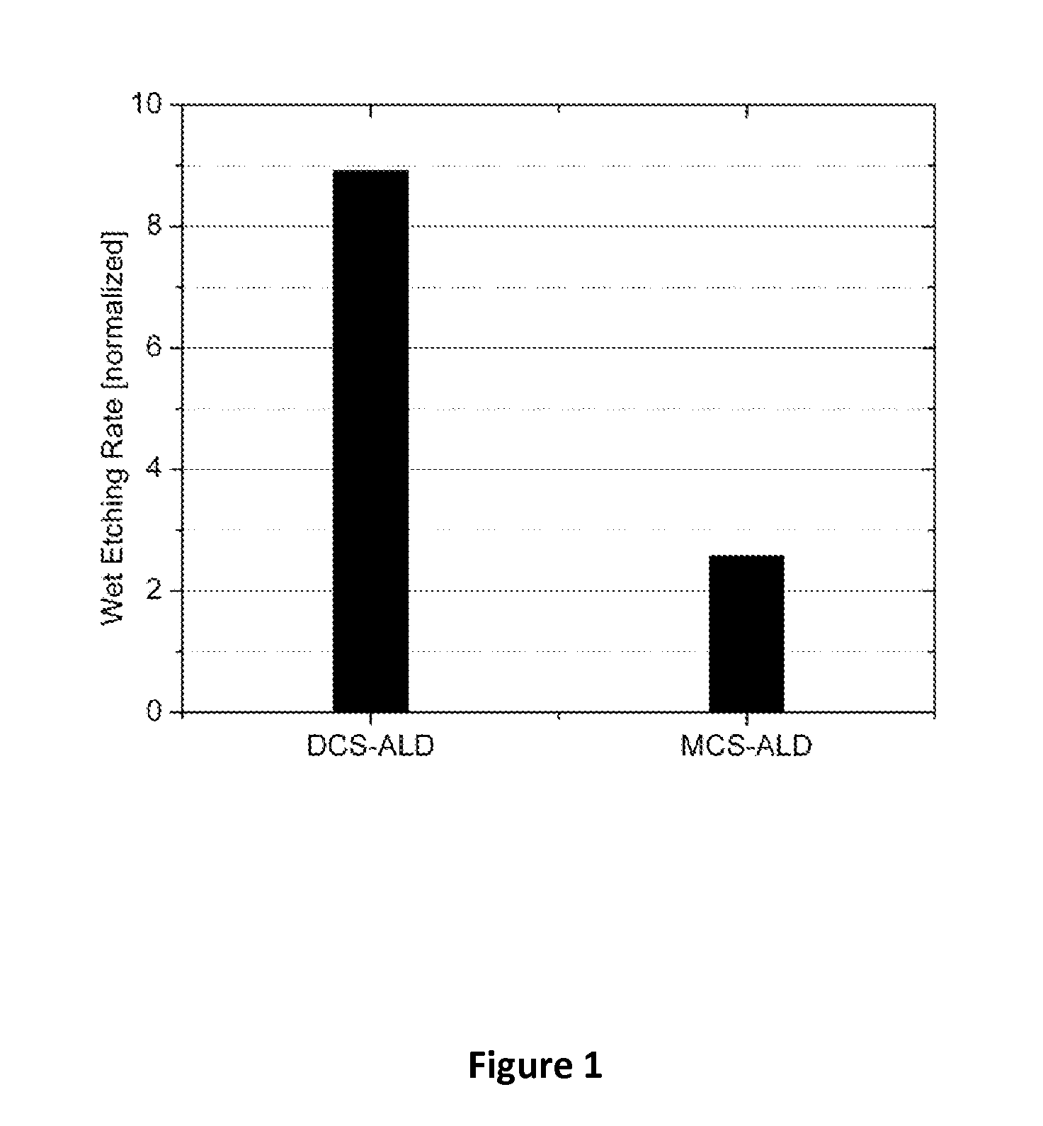
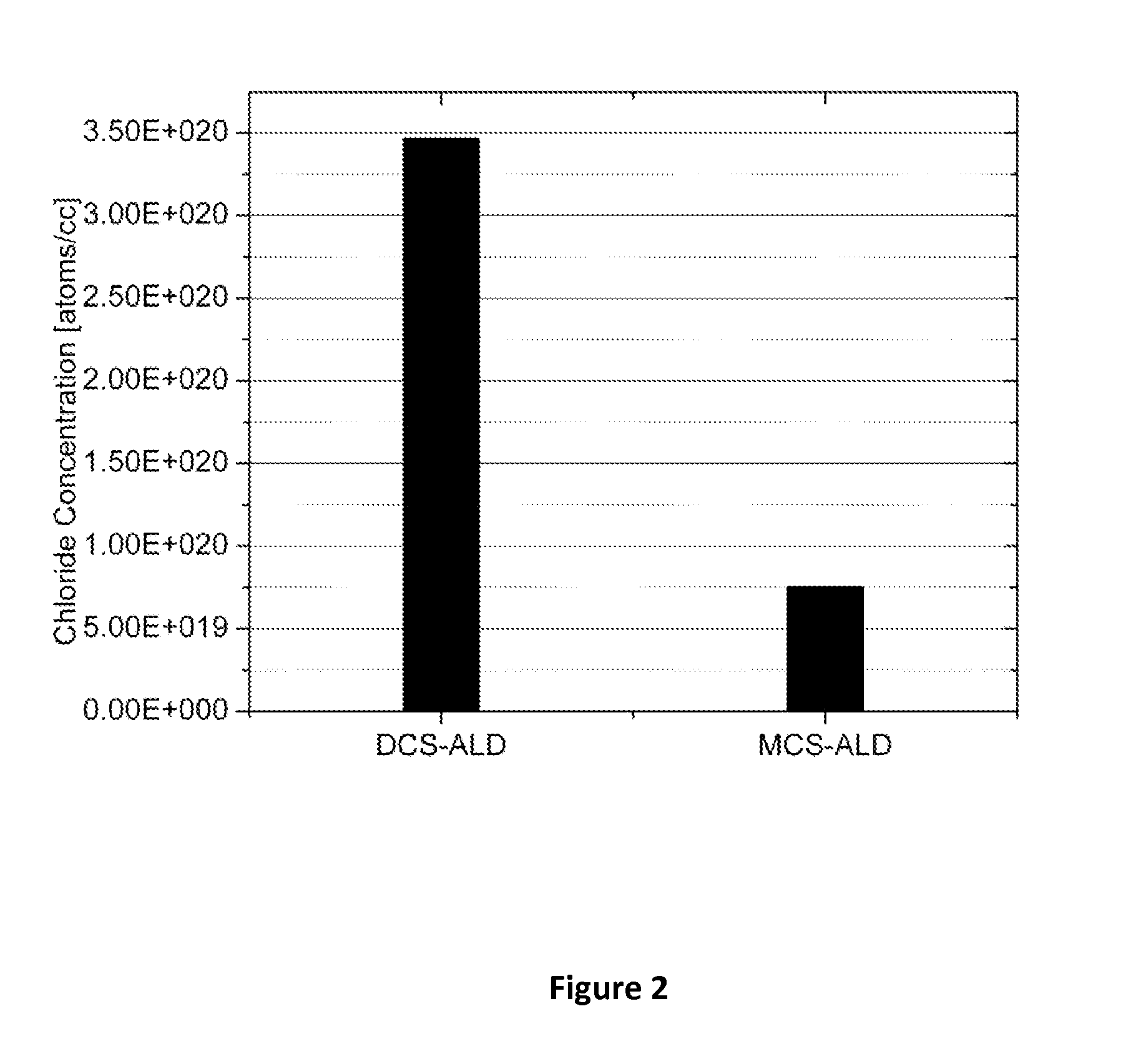
[0031]MCS (monochlorosilane) as the Si precursor was introduced to the reactor at a fixed flow rate. The reactor was saturated with MCS for a short fixed time (typically 10 seconds), and then pumped down to 0.1 T, followed by introducing a fixed flow of NH3. The reactor was again pumped down after NH3 precursor saturation for a short fixed time (typically 20 seconds). This cycle is repeated until desired film thickness is achieved.

[0032]The plasma power was set at approximately 100 W, and the temperature was set at approximately 450° C.

[0033]The plasma can be a nitrogen plasma, a mixture of nitrogen and...

embodiment 1

Silicon Oxide Film

[0036]In this embodiment, a method of forming silicon oxide films comprises the following steps.

[0037]Substrates to be deposited films on are loaded to a hot wall CVD or ALD reactor. The reactor is flashed with Ar and pumped down to low pressure of less than 2 Torr (T) and heated up to a temperature at which film deposition is performed.

[0038]For CVD process, a fixed flow rate of MCS (monochlorosilane) as the Si precursor is introduced to the reactor. A fixed flow of a fixed flow of ozone as oxygen precursor is introduced to the reactor at the same time as MCS. The flow stops and then the deposition process stops when a desired film thickness is reached.

[0039]For ALD or cyclic CVD process, a fixed flow rate of MCS (monochlorosilane) as the Si precursor is introduced to the reactor. The reactor is saturated with MCS for a short fixed time (typical less than 10 seconds), and then pumped down to 2 T, followed by introducing a fixed flow of ozone, or a plasma excited O...

embodiment 2

Silicon Oxynitride Film

[0042]In this embodiment, a method of forming silicon oxynitride films comprises the following steps.

[0043]Substrates to be deposited films on are loaded to a hot wall CVD or ALD reactor. The reactor is flashed with Ar and pumped down to low pressure of less than 2 T and heated up to a temperature at which film deposition is performed;

[0044]For CVD process, a fixed flow rate of MCS (monochlorosilane) as the Si precursor is introduced to the reactor. A fixed flow of nitrogen source such as NH3 and a fixed flow of O2 as oxygen precursor are introduced to the reactor at the same time as MCS. The flow stops and then the deposition process stops when a desired film thickness is reached.

[0045]For ALD or cyclic CVD process, a fixed flow rate of MCS (monochlorosilane) as the Si precursor is introduced to the reactor. The reactor is saturated with MCS for a short fixed time (typical less than 10 seconds), and then pumped down to 2 T, followed by introducing a fixed flo...


PUM

PropertyMeasurementUnit
temperaturesaaaaaaaaaa
pressureaaaaaaaaaa

Abstract

This invention discloses the method of forming silicon nitride, silicon oxynitride, silicon oxide, carbon-doped silicon nitride, carbon-doped silicon oxide and carbon-doped oxynitride films at low deposition temperatures. The silicon containing precursors used for the deposition are monochlorosilane (MCS) and monochloroalkylsilanes. The method is preferably carried out by using plasma enhanced atomic layer deposition, plasma enhanced chemical vapor deposition, and plasma enhanced cyclic chemical vapor deposition.

Description

CROSS-REFERENCE TO RELATED APPLICATIONS[0001]This application claims benefit of U.S. Provisional Application No. 61 / 057,891, filed Jun. 2, 2008 and U.S. Provisional Application No. 61 / 058,374, filed Jun. 3, 2008. The disclosures of those provisional applications are hereby incorporated by reference.BACKGROUND OF THE INVENTION[0002]Thin films of silicon nitride have been widely used in various applications due to their unique physical, chemical and mechanical properties. In semiconductor devices particularly, silicon nitride films are used as gate insulations, diffusion masks, sidewall spacers, passivation and encapsulation, etc. Typically, silicon nitride films used in the Front End of Line (FEOL) are currently deposited by Low pressure chemical vapor deposition (LPCVD) in a hot wall reactor at >750° C. using dichlorosilane and ammonia. As the lateral and vertical dimensions of Integrate Circuit (IC) continue to shrink, however, there is an increasing demand for silicon nitride f...

Claims


Application Information

Patent Timeline
Patent Type & Authority Applications(United States)
IPC IPC(8): H05H1/24B05D5/12
CPCC23C16/308C23C16/345C23C16/401C23C16/45536H01L21/02126H01L21/0214H01L21/02164H01L21/0217H01L21/02211H01L21/02274H01L21/0228H01L21/3145H01L21/31608H01L21/31633H01L21/3185H01L21/02271H01L21/02263
Inventor YANG, LIULEI, XINJIANHAN, BINGXIAO, MANCHAOKARWACKI, JR., EUGENE JOSEPHHASEBE, KAZUHIDEMATSUNAGA, MASANOBUYONEZAWA, MASATOCHENG, HANSONG
Owner TOKYO ELECTRON LTD
Why Eureka
Try Eureka