Organic light-emitting device (OLED) packaging structure and method

An electroluminescent device and packaging structure technology, which is applied in the direction of electro-solid devices, electrical components, semiconductor devices, etc., can solve the problems of different efficiency, slow deposition speed, etc. Effect

Inactive Publication Date: 2016-06-15
NO 55 INST CHINA ELECTRONIC SCI & TECHNOLOGYGROUP CO LTD
View PDF8 Cites 14 Cited by
  • Summary
  • Abstract
  • Description
  • Claims
  • Application Information

AI Technical Summary

Problems solved by technology

[0004] The purpose of the present invention is to solve the problem of slow deposition rate and different efficiency in the existing atomic layer deposition packaging technology, and to invent an effective packaging film that can improve the production efficiency of the packaging film and reduce the time-consuming packaging process while obtaining good water vapor barrier performance. Encapsulation structure and encapsulation method of electromechanical luminescent device

Method used


Image

  • Organic light-emitting device (OLED) packaging structure and method
  • Organic light-emitting device (OLED) packaging structure and method

Examples


Embodiment 1

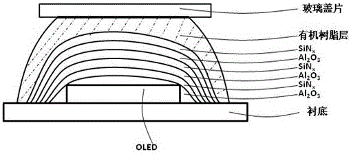
[0032] Such as figure 1 shown.

[0033] A packaging structure of an organic electroluminescent device, which is mainly composed of a substrate substrate, an OLED light-emitting element, a thin film packaging layer, an organic resin layer and a glass cover sheet, and is formed by the following packaging method:

[0034] (1) Form OLED on the base substrate;

[0035] (2) Forming Al on the OLED substrate by atomic layer deposition 2 o 3 film, the precursors used in the deposition process are trimethylaluminum (TMA) and water vapor (H 2 O), injected with nitrogen (N 2 ) as a purge gas; the injection time of trimethylaluminum is 0.02s, the injection time of water vapor is 0.02s, and the injection time of nitrogen is 30s; the chamber pressure is 20Pa, and the deposition temperature is 80°C; Al 2 o 3 The thickness of the film is 30nm;

[0036] (3) in Al 2 o 3Formation of SiN on thin film surface by plasma-enhanced chemical vapor deposition x film, the gas source used in the ...

Embodiment 2

[0042] Such as figure 1 As shown, a packaging structure of an organic electroluminescent device, which sequentially includes a base substrate, an OLED light-emitting element, a thin film packaging layer, an organic resin layer and a glass cover.

[0043] Specifically, the packaging method in this embodiment includes the following steps:

[0044] (1), (2) are the same as embodiment one;

[0045] (3) in Al 2 o 3 SiN is formed on the surface of the film by sputtering x Thin film, the target in the deposition process is a silicon target with a purity of 99.99%, and the background vacuum is 8×10 -4 Pa, the sputtering gas is 99.99% nitrogen and argon respectively, the sputtering power is 400W, the reaction pressure is 0.5Pa, the flow rate of nitrogen gas is 40sccm, and the flow rate of argon gas is 60sccm; SiN x The thickness of the film is 1200nm;

[0046] Steps (4), (5), and (6) steps are the same as in Embodiment 1;

[0047] The water vapor permeability (WVTR) of the OLED ...

Embodiment 3

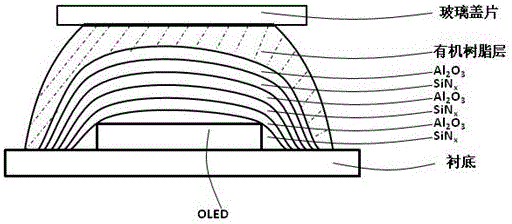
[0049] figure 2 shown.

[0050] A packaging structure of an organic electroluminescent device, which includes a base substrate, an OLED light-emitting element, a thin film packaging layer, an organic resin layer and a glass cover sheet.

[0051] Specifically, the packaging method in this embodiment includes the following steps:

[0052] (1) Form OLED on the base substrate;

[0053] (2) SiN is prepared by plasma-enhanced chemical vapor deposition method on the substrate substrate forming OLED x film, the gas source used in the deposition process is silane (SiH 4 ) and ammonia (NH 3 ), the flow rate of silane is 20sccm, and the flow rate of ammonia gas is 190sccm; the working pressure is 10Pa, and the power is 60W; SiN x The thickness of the film is 1500nm;

[0054] (3) in SiN x Al was formed on the surface of the film by atomic layer deposition 2 o 3 film, the precursors used in the deposition process are trimethylaluminum (TMA) and water vapor (H 2 O), injected with...


PUM


Abstract

The invention discloses an organic light-emitting device (OLED) packaging structure and a method. The packaging structure is characterized by comprising a substrate, the OLED, a thin film packaging layer, an organic resin layer and a glass cover sheet, wherein Al2O3 thin films and SiNx thin films are sequentially overlapped to form the thin film packaging layer. In the packaging method, the Al2O3 thin film is prepared by using an atomic layer deposition technology, the SiNx thin film is prepared by using a plasma chemical vapor deposition or sputtering technology, and thus, the thin film packaging layer has high compactness, water vapor can be prevented from corroding the OLED, and the thin film packaging layer making efficiency is also improved. As the organic resin layer and the glass cover sheet are arranged on the thin film packaging layer, by using the full covering effects of the organic resin layer and the protection effects of the glass cover sheet, the service life of the device is further improved.

Description

technical field [0001] The invention relates to display technology, in particular to an organic electroluminescent device technology, in particular to a packaging structure and a packaging method for an organic electroluminescent device. Background technique [0002] At present, organic electroluminescent devices (OLEDs) have attracted extensive attention from academia and business circles due to their advantages such as self-luminescence, low energy consumption, wide viewing angle, fast response speed, and flexibility. At present, as major manufacturers in the display industry continue to invest a lot of money in technology research and development, OLED flat panel display technology is at a critical stage where mass production technology is maturing and market demand is growing rapidly. Since OLEDs are particularly sensitive to water vapor and oxygen in the environment, the water vapor and oxygen infiltrating into the device will corrode electrodes and organic layer materi...

Claims


Application Information

Patent Timeline
Patent Type & Authority Applications(China)
IPC IPC(8): H01L51/52H01L51/56
CPCH10K71/00H10K50/84
Inventor 杨建兵吴远武邹成杨洪宝洪乙又樊卫华王绪丰
Owner NO 55 INST CHINA ELECTRONIC SCI & TECHNOLOGYGROUP CO LTD
Why Eureka
Try Eureka