Preparation method for organic silicon nanometer hard protective coating

A protective coating and nano-coating technology, which is applied in coatings, metal material coating processes, gaseous chemical plating, etc., can solve problems such as poor controllability of coating thickness, adverse effects of electronic products, and difficulty in controlling nano-levels , to achieve the effect of improving protection performance, improving compactness and speed

Active Publication Date: 2017-12-29
JIANGSU FAVORED NANOTECHNOLOGY CO LTD
View PDF7 Cites 14 Cited by
  • Summary
  • Abstract
  • Description
  • Claims
  • Application Information

AI Technical Summary

Problems solved by technology

[0019] (1) It is necessary to use water or organic substances as solvents, which have adverse effects on electronic products;
[0020] (2) There is waste water, waste liquid and waste gas, and post-treatment is required;
[0021] (3) The controllability of the coating thickness is poor, and it is difficult to control it to the nanometer level
[0022] In addition, the current organic coatings obtained by plasma deposition, such as fluorocarbon coatings, parylene coatings, etc., usually have a hardness of HB-2H, which is easy to cause damage under touching and scratching conditions, reducing the service life

Method used


Image

  • Preparation method for organic silicon nanometer hard protective coating
  • Preparation method for organic silicon nanometer hard protective coating
  • Preparation method for organic silicon nanometer hard protective coating

Examples


Embodiment 1

[0091] A preparation method of organosilicon hard nano protective coating, comprising the following steps:

[0092] (1) Pre-processing:

[0093] Place the substrate in the reaction chamber of the nano-coating preparation equipment, close the reaction chamber and continuously evacuate the reaction chamber, pump the vacuum in the reaction chamber to 10 mTorr, pass in the inert gas Ar, and open the movement mechanism , causing the substrate to move in the reaction chamber;

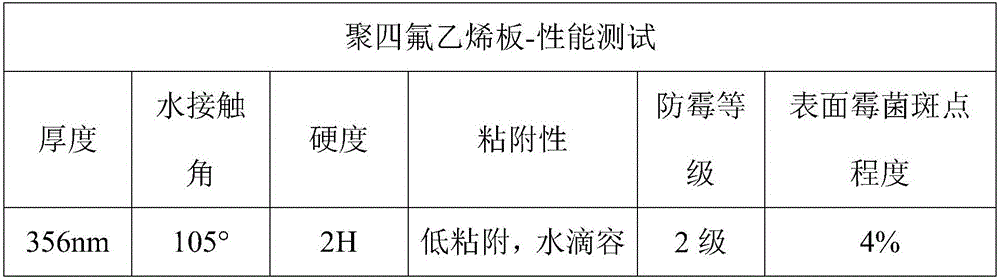
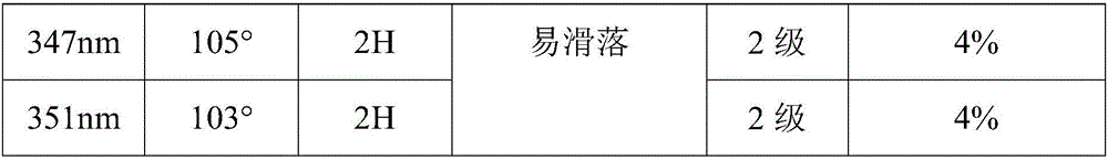
[0094] In step (1), the base material is a solid material, and the solid material is a block-shaped polytetrafluoroethylene plate.

[0095] In the step (1), the reaction chamber is a rotating chamber, the volume of the reaction chamber is 50 L, the temperature of the reaction chamber is controlled at 30° C., and the flow rate of the inert gas is 5 sccm.

[0096] In step (1), the substrate moves in the reaction chamber, and the substrate moves in a circular motion relative to the reaction chamber at a speed ...

Embodiment 2

[0116] A preparation method of organosilicon hard nano protective coating, comprising the following steps:

[0117] (1) Pre-processing:

[0118] Place the substrate in the reaction chamber of the nano-coating preparation equipment, close the reaction chamber and continuously evacuate the reaction chamber, evacuate the vacuum in the reaction chamber to 60 millitorr, feed inert gas He, start the movement mechanism, move the substrate;

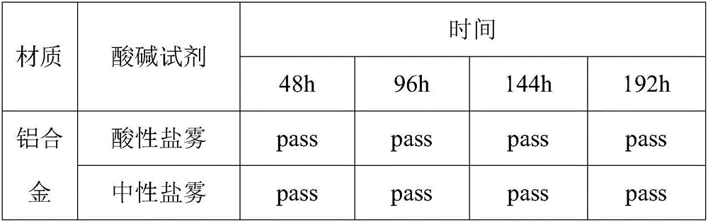
[0119] In step (1), the base material is a solid material, and the solid material is a block aluminum alloy material.

[0120] In step (1), the reaction chamber is a cubic chamber with a volume of 250 L, the temperature of the reaction chamber is controlled at 43° C., and the flow rate of the inert gas is 18 sccm.

[0121] In step (1), the base material performs planetary motion, with a revolution speed of 2 revolutions / min and an autorotation speed of 6 revolutions / min.

[0122] (2) Silicone coating preparation:

[0123] Introduce monomer va...

Embodiment 3

[0141] A preparation method of organosilicon hard nano protective coating, comprising the following steps:

[0142] (1) Pre-processing:

[0143] Place the substrate in the reaction chamber of the nano-coating preparation equipment, close the reaction chamber and continuously evacuate the reaction chamber, pump the vacuum in the reaction chamber to 130 mTorr, and introduce a mixture of inert gases Ar and He The gas activates the movement mechanism to make the substrate move;

[0144] In step (1), the base material is a solid material, and the solid material is a bulk alloy steel plate material.

[0145] In the step (1), the reaction chamber is a rotating chamber, the volume of the reaction chamber is 480L, the temperature of the reaction chamber is controlled at 50° C., and the flow rate of the inert gas is 80 sccm.

[0146] In step (1), the base material performs circular motion at a speed of 8 revolutions / min.

[0147] (2) Silicone coating preparation:

[0148] Introduce ...


PUM

PropertyMeasurementUnit
hardnessaaaaaaaaaa
poweraaaaaaaaaa
hardnessaaaaaaaaaa

Abstract

The invention discloses a preparation method for an organic silicon nanometer hard protective coating, and belongs to the technical field of plasmas. In the method, a reaction chamber is vacuumized, an inert gas is charged to enable a base material to move, monomer steam is charged, chemical vapor deposition is carried out, and an organic silicon nanometer coating is prepared on the surface of the base material through the chemical vapor deposition; and the component of the monomer steam is the mixture of at least one organic silicon monomer containing double bonds and a Si-Cl structure or a Si-O-C structure or a Si-N-Si structure or a Si-O-Si structure or a cyclic structure, and at least one polyfunctional unsaturated hydrocarbon and hydrocarbon derivative, charging for the monomer steam is stopped, oxygen and/or vapor is charged, and hard treatment is carried out on the surface of the organic silicon nanometer coating. According to the preparation method disclosed by the invention, the traditional organic carbonate hydroxide compound monomer is replaced by the organic silicon monomer, each silicon atom at least provides 1-4 active sites, high activity is achieved, a part of oxygen is introduced into the monomer, organic silicon can be oxidized into nanometer silicon dioxide, and the hardness of the coating can be greatly increased due to a dispersion strengthening effect.

Description

technical field [0001] The invention belongs to the technical field of plasma chemical vapor deposition, and in particular relates to a preparation method of an organosilicon nano protective coating. Background technique [0002] Anti-mold, anti-humidity, and anti-salt mist (referred to as three antis) are important problems that need to be solved during the storage, transportation and use of electronic devices. Mold, salt spray and humidity often cause electronic devices to fail due to short circuits. Therefore, coating protective coatings on the surface of electronic products is an important method to improve the service life of electronic products. As the types of electronic products continue to increase, more and more electronic devices need to be touched and operated, so that the protective coating is damaged by external force, resulting in a decrease in the protective performance of the coating. Therefore, for the protective coating used in the electronics industry, ...

Claims


Application Information

Patent Timeline
Patent Type & Authority Applications(China)
IPC IPC(8): C23C16/513C23C16/448C23C16/56
CPCC23C16/448C23C16/513C23C16/56
Inventor 宗坚
Owner JIANGSU FAVORED NANOTECHNOLOGY CO LTD
Why Eureka
Try Eureka