Method for preparing efficient thin-film solar cell light absorption layer

A technology for solar cells and light absorbing layers, which is applied in the manufacturing of circuits, electrical components, and final products, etc., can solve the problems of affecting CIGS preparation, poor preparation uniformity, and high environmental protection costs, and achieves low cost, simple equipment, and low deposition temperature. Effect

Inactive Publication Date: 2009-09-09
上海纳晶科技有限公司
View PDF0 Cites 13 Cited by
  • Summary
  • Abstract
  • Description
  • Claims
  • Application Information

AI Technical Summary

Problems solved by technology

[0004] CIGS solar cells prepared by methods such as magnetron sputtering, co-evaporation, and electroplating in the prior art have higher conversion efficiency, but a high-vacuum system is required to prepare thin films, the cost is higher, and the uniformity of large-area preparation is relatively poor. Selenium ( Sulfur) process temperature is higher (400-550 ° C), and the H used in the selenium (sulfur) process 2 Se(H 2 S) or Se(S) are highly toxic substances with high environmental protection costs, and the operation requirements for their preservation and use are relatively strict, which seriously affects the preparation of CIGS

Method used


Image

  • Method for preparing efficient thin-film solar cell light absorption layer
  • Method for preparing efficient thin-film solar cell light absorption layer
  • Method for preparing efficient thin-film solar cell light absorption layer

Examples


Embodiment 1

[0021] First, the following solutions were prepared respectively in a nitrogen protective atmosphere:

[0022] Prepare solution A: weigh 1.283g Cu 2 S, 0.512g S was added to 16mL of hydrazine solution, after 10h of stirring reaction, it was allowed to stand still to form a clear yellow solution A;

[0023] Preparation of colorless solution B: Dissolve 2.486 g of In 2 Se 3 Prepared by dissolving 0.421g Se in 16mL of hydrazine solution;

[0024] Prepare solution C: Dissolve 1.264g of Se in 8mL of hydrazine and react;

[0025] Preparation of solution D: Continue to weigh 0.561g Ga and 1.264g Se into 16mL of hydrazine solution to obtain colorless solution D.

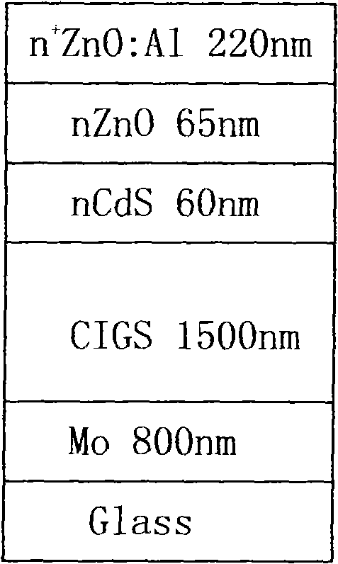
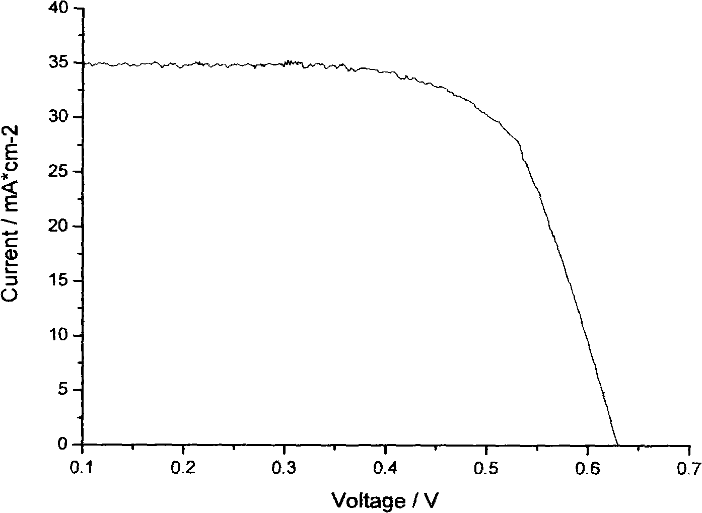
[0026] Then, pipette 2.0mL of solution A, 2.3mL of solution B, 2.5mL of solution C and 1.2mL of solution D, mix them and put them into a dry container. Coated on a Mo-coated glass substrate, after heat treatment at 300°C for 10 minutes, the temperature was raised to 450-550°C at a rate of 10-25°C / min, and kept for 45 mi...

Embodiment 2

[0028] First, the following solutions were prepared respectively in a nitrogen protective atmosphere:

[0029] Prepare solution A: weigh 0.803g of Cu 2 S, 0.321g of S was added to 10mL of hydrazine solution, stirred and reacted for 10h, and left to form solution A;

[0030] Preparation of solution B: 2.3411 g of In 2 Se 3 Prepared by dissolving 0.395g of Se in 10mL of hydrazine solution;

[0031] Prepare solution C: Dissolve 0.956g of Se in 5mL of hydrazine and react.

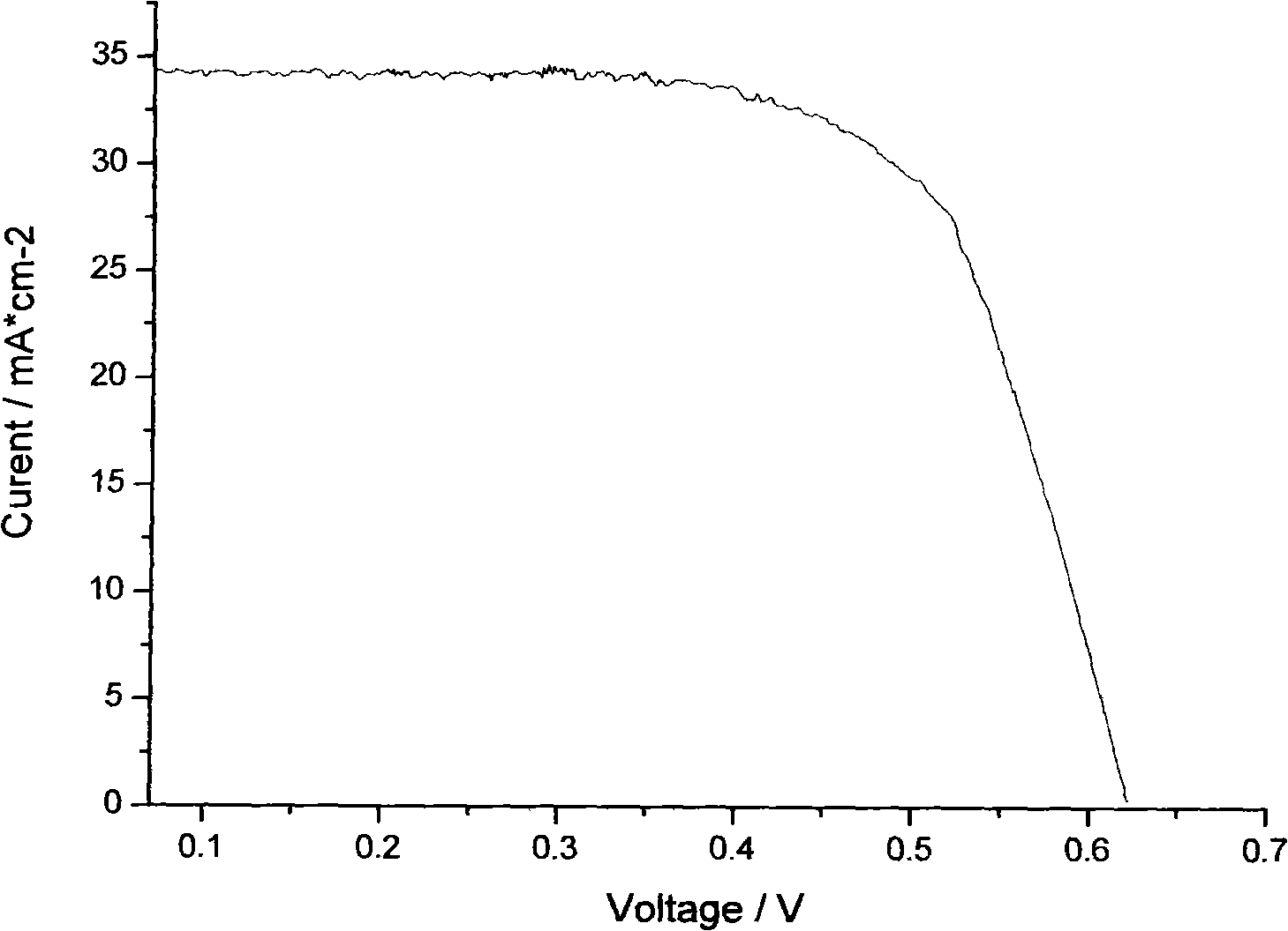
[0032] Then, pipette 2.0mL of solution A, 2.0mL of solution B, and 2.4mL of solution C, mix them into a dry container, and after fully stirring and filtering, apply the spray method to the Mo-coated glass substrate in a nitrogen atmosphere. After heat treatment at a constant temperature of 300°C for 5 minutes, the temperature was raised to 450-550°C at a rate of 10-25°C / min and kept for 45 minutes to finally obtain CuInSe 2 Thin film, i.e. copper indium selenium thin film, adopts the copper indium gallium ...

Embodiment 3

[0034] First, the following solutions were prepared respectively in a nitrogen protective atmosphere:

[0035] Prepare solution A: weigh 0.955g of Cu 2 S and 0.382g of S were added to 12mL of hydrazine solution, stirred and reacted for 10h, and left to form solution A;

[0036] Preparation of solution B: 1.9434 g of In 2 S 3 Prepared by dissolving 0.1909g of S in 12mL of hydrazine solution;

[0037] Prepare solution C: Dissolve 0.384g of S in 6mL of hydrazine and react.

[0038] Then, pipette 4.0mL of solution A, 4.0mL of solution B, and 1.6mL of solution C respectively, mix them into a dry container, and after fully stirring and filtering, apply spray coating on a Mo-coated glass substrate in a nitrogen atmosphere. After heat treatment at 300°C for 5 minutes, the temperature was raised to 450-550°C at a rate of 10-25°C / min, and kept for 45 minutes to obtain CuInS 2 Thin film, i.e. copper indium sulfur thin film, adopts the copper indium gallium selenium thin film prepare...


PUM


Abstract

The invention relates to the technical field of photovoltaic new energy in semiconductive thin film preparation, in particular to a method for preparing an efficient thin-film solar cell light absorption layer. The method comprises the following steps: Cu2S and S are added to hydrazine solution and evenly mixed to obtain solution A; In2Se3 and Se or In2Se3 and the S are added to the hydrazine solution to obtain solution B; the Se and the S are added to the hydrazine solution to obtain solution C; Ga and the Se or Ga and the S are added to the hydrazine solution to obtain solution D; the prepared solution A, solution B, solution C and solution D or the solution A, the solution B and the solution C are mixed to prepare reactive precursor solution; and then the precursor solution is coated on a conducting substrate by a physical method to prepare a CIGS thin film. Compared with the prior art, the method has simple process; can help accurately adjust and control the proportions of various metal atoms in the absorption layer, ensure 14-18% of higher photoelectric conversion efficiency and avoid selenylation or vulcanization post-processing process.

Description

[technical field] [0001] The invention relates to the technical field of photovoltaic new energy in the preparation of semiconductor thin films, in particular to a method for preparing a light-absorbing layer of a high-efficiency thin-film solar cell. [Background technique] [0002] Copper indium (gallium) selenium (sulfur) including copper indium gallium selenide (Cu(In, Ga)Se 2 ), Copper Indium Selenium (CuInSe 2 ) or copper indium gallium sulfide (Cu(In, Ga)S 2 ), copper indium sulfide (CuInS 2 ) thin film (collectively referred to as CIGS) solar cell is a new type of compound semiconductor solar cell developed in the late 1980s. The typical structure of CIGS battery is: glass (stainless steel) substrate, back electrode layer (Mo), absorber layer (CIGS), buffer layer (CdS), ZnO window layer with double-layer structure, intrinsic ZnO (i-ZnO) layer , Al-doped low-resistance transparent ZnO (Al:ZnO) layer and aluminum electrodes. Among them, the CIGS thin film is the li...

Claims


Application Information

Patent Timeline
Patent Type & Authority Applications(China)
IPC IPC(8): H01L31/18
CPCY02P70/50
Inventor 潘丽坤曹美玲林丽锋
Owner 上海纳晶科技有限公司
Why Eureka
Try Eureka