Forming capping layer over metal wire structure using selective atomic layer deposition

a technology of atomic layer deposition and capping layer, which is applied in the direction of semiconductor devices, semiconductor/solid-state device details, material nanotechnology, etc., can solve the problems of current leakage and device failure, formation of “voids” in the conductor that can grow to a size, and complicated structur

Inactive Publication Date: 2006-08-01
IBM CORP
View PDF15 Cites 444 Cited by
  • Summary
  • Abstract
  • Description
  • Claims
  • Application Information

AI Technical Summary

Problems solved by technology

Metal migration is the diffusion of molecules of a metal conductor (such as copper or aluminum) into surrounding dielectric such as silicon dioxide or polymers from exposure to high temperatures, which ultimately leads to current leakage and device failure.
Electromigration is the movement of atoms of a metal conductor in response to the passage of h

Method used


Image

  • Forming capping layer over metal wire structure using selective atomic layer deposition
  • Forming capping layer over metal wire structure using selective atomic layer deposition
  • Forming capping layer over metal wire structure using selective atomic layer deposition

Examples


Embodiment Construction

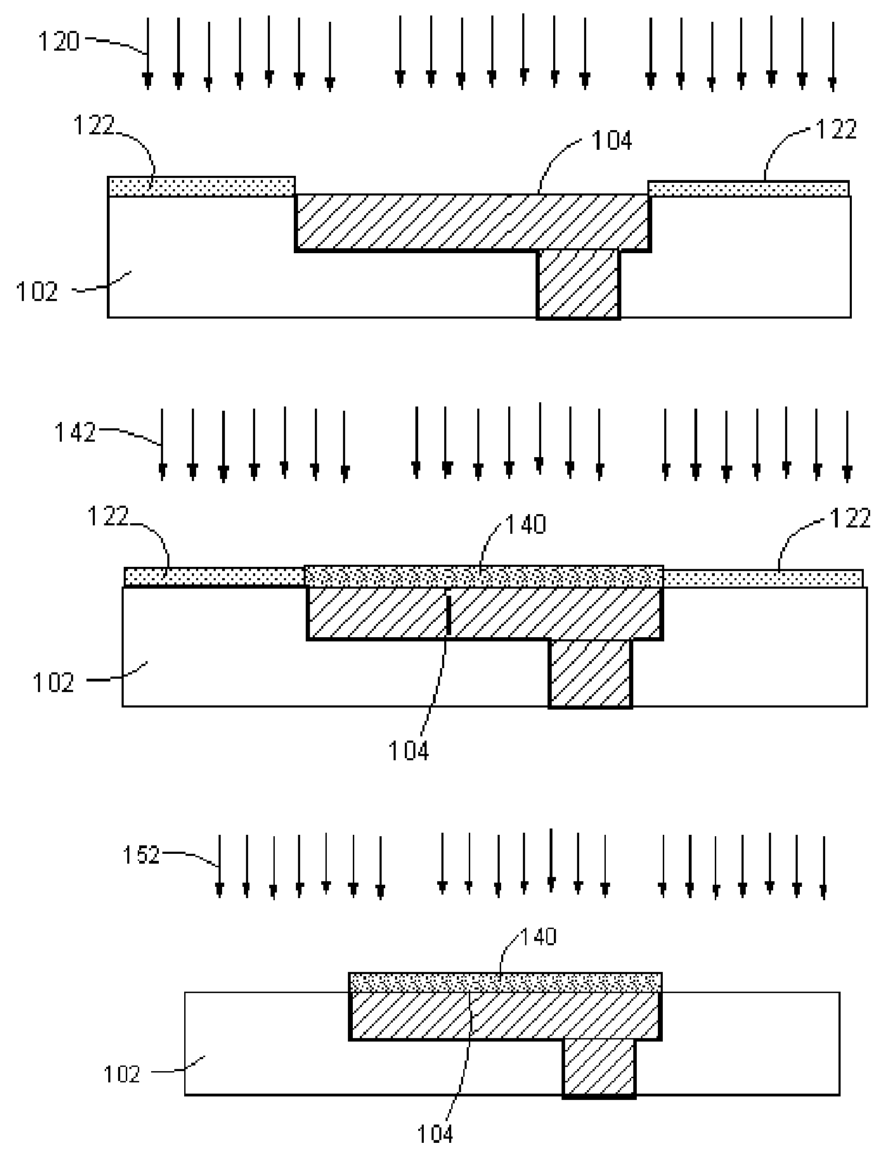
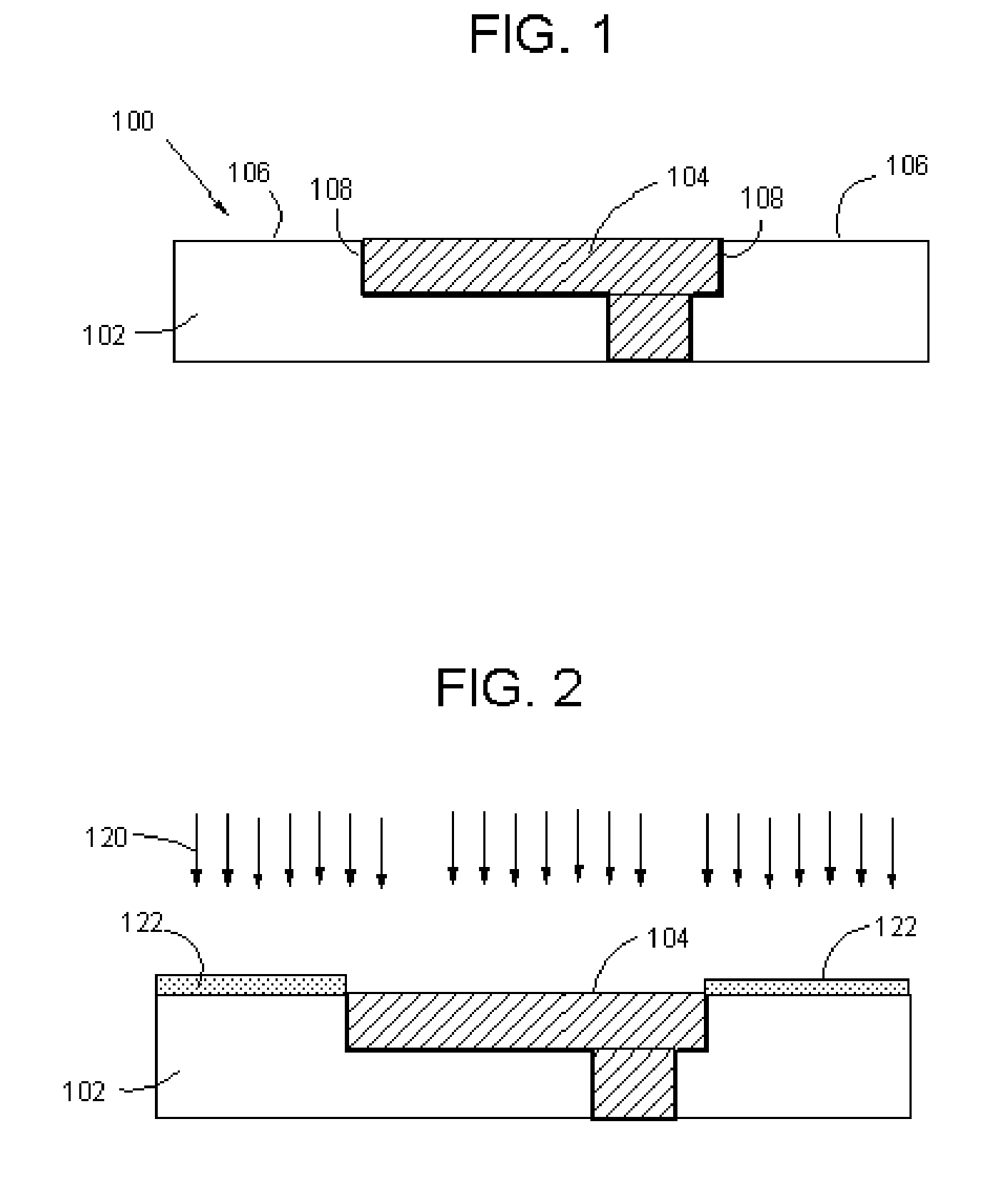
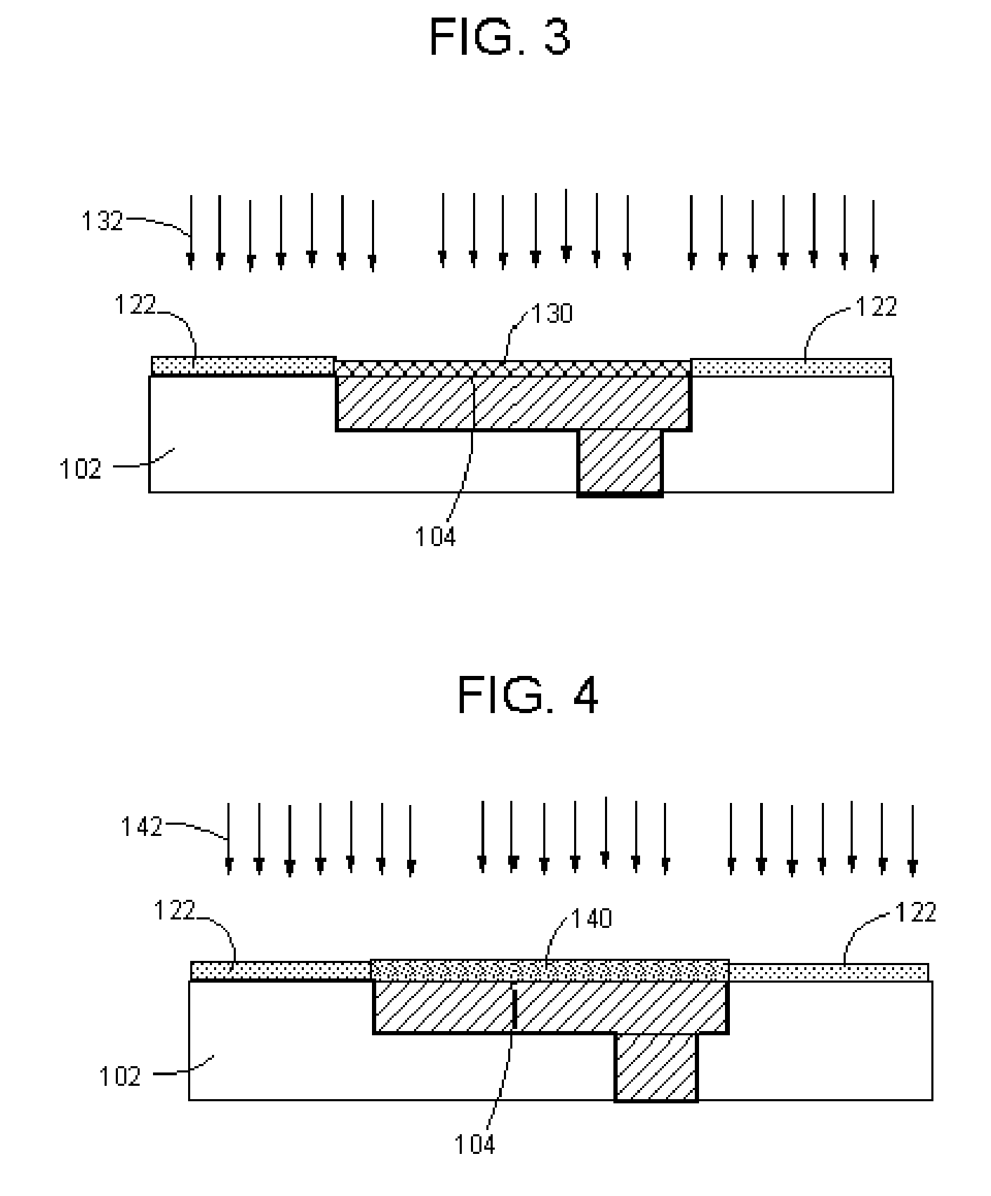
[0018]With reference to the accompanying drawings, FIG. 1 shows a first step of one embodiment of a method of forming a capping layer over a metal wire structure of a semiconductor device. As shown in FIG. 1, a partially fabricated semiconductor device 100 is provided. Device 100 has been processed up through a wiring mask level, dielectric etch, liner deposition, metal fill in a dielectric 102, and chemical mechanical polishing (CMP) to planarize a metal wire structure 104. At this point, device 100 includes exposed surfaces of metal wire structure 104 and an exposed surface 106 of dielectric 102 that extends around metal wire structure 104. Liners 108 may be provided about metal wire structure 104, and also have upper surfaces thereof exposed at this point. Metal wire structure 104 may include copper (Cu), aluminum (Al) or other metal conductor(s). In one preferred embodiment, however, metal wire structure 104 includes copper (Cu). Dielectric 102 may include a silicon dioxide (SiO...


PUM


Abstract

Methods of forming a capping layer over a metal wire structure of a semiconductor device are disclosed. In one embodiment, the method includes providing a partially fabricated semiconductor device having exposed surfaces of the metal (e.g., copper) wire structure and a dielectric around the metal wire structure. The exposed surface of the metal wire structure is then activated by forming a seed layer thereon. The capping layer is then formed over the exposed surface of the metal wire structure by performing a selective atomic layer deposition (ALD) of a capping layer material onto the metal wire structure. As an alternative, the dielectric may be masked off to further assist the selectivity of the ALD. The invention also includes a semiconductor structure including the metal wire structure having an atomic layer deposition capping layer over an upper surface thereof.

Description

BACKGROUND OF THE INVENTION[0001]1. Technical Field[0002]The present invention relates generally to semiconductor fabrication, and more particularly, to forming a capping layer over a metal wire structure in a partially fabricated semiconductor device using selective atomic layer deposition.[0003]2. Related Art[0004]Metal migration is the diffusion of molecules of a metal conductor (such as copper or aluminum) into surrounding dielectric such as silicon dioxide or polymers from exposure to high temperatures, which ultimately leads to current leakage and device failure. Electromigration is the movement of atoms of a metal conductor in response to the passage of high current through it, which can lead to the formation of “voids” in the conductor that can grow to a size where the conductor is unable to pass current. Typically, metal migration and electromigration have been addressed by providing liners about metal conductors; these liners hinder or forestall these effects.[0005]One cha...

Claims


Application Information

Patent Timeline
IPC IPC(8): H01L21/44
CPCB82Y30/00H01L21/3105H01L21/316H01L21/76826H01L21/76828H01L21/76834H01L21/76849H01L21/76855H01L21/76867H01L21/76876H01L21/76829Y10S438/902H01L21/02205H01L21/02183H01L21/02189H01L21/0228H01L21/02178H01L21/02181H01L21/02186
Inventor FURUKAWA, TOSHIHARUHOLMES, STEVEN J.HORAK, DAVID V.KOBURGER, III, CHARLES W.
Owner IBM CORP
Why Eureka
Try Eureka