Array substrate and method for driving the same

a technology of array substrate and array electrode, which is applied in the field of display, can solve the problems of increasing the cost of producing array substrate and the need for double charge of pixel electrode, and achieve the effect of maintaining the charging efficiency of pixel electrode and reducing the cost of producing liquid crystal panel

Inactive Publication Date: 2018-08-14
TCL CHINA STAR OPTOELECTRONICS TECH CO LTD
View PDF26 Cites 0 Cited by
  • Summary
  • Abstract
  • Description
  • Claims
  • Application Information

AI Technical Summary

Benefits of technology

[0007]In order to solve the above problem, the present disclosure provides an array substrate and a corresponding method for driving the array substrate, which can maintain the charging efficiency of the pixel electrode and at the same time reduce the cost for producing the liquid crystal panel.
[0026]According to the present disclosure, a scan signal of a scan line enables the first TFT switches of the pixel units in a line, and at the same time enables the second TFT switches of the pixel units in another line. In this case, the number of scan lines needed for enabling the TFT switches on is reduced, and thus the chips for driving the scan lines can be reduced, thereby the cost of producing the array substrate can be reduced.

Problems solved by technology

Due to the limitation of the manufacturing technology, impurities would mix in the liquid crystal molecules.
However, such driving method would lead to reversal inversion of the signal, causing the charge needed for the pixel electrode to double.
Under such circumstances, more driving chips of the scan lines are needed, thereby increasing the cost of producing the array substrate.

Method used


Image

  • Array substrate and method for driving the same
  • Array substrate and method for driving the same
  • Array substrate and method for driving the same

Examples


Embodiment Construction

[0035]The present disclosure will be explained in detail with reference to the embodiments and the accompanying drawings, whereby it can be fully understood how to solve the technical problem by the technical means according to the present disclosure and achieve the technical effects thereof, and thus the technical solution according to the present disclosure can be implemented. It is important to note that as long as there is no structural conflict, all the technical features mentioned in all the embodiments may be combined together in any manner, and the technical solutions obtained in this manner all fall within the scope of the present disclosure.

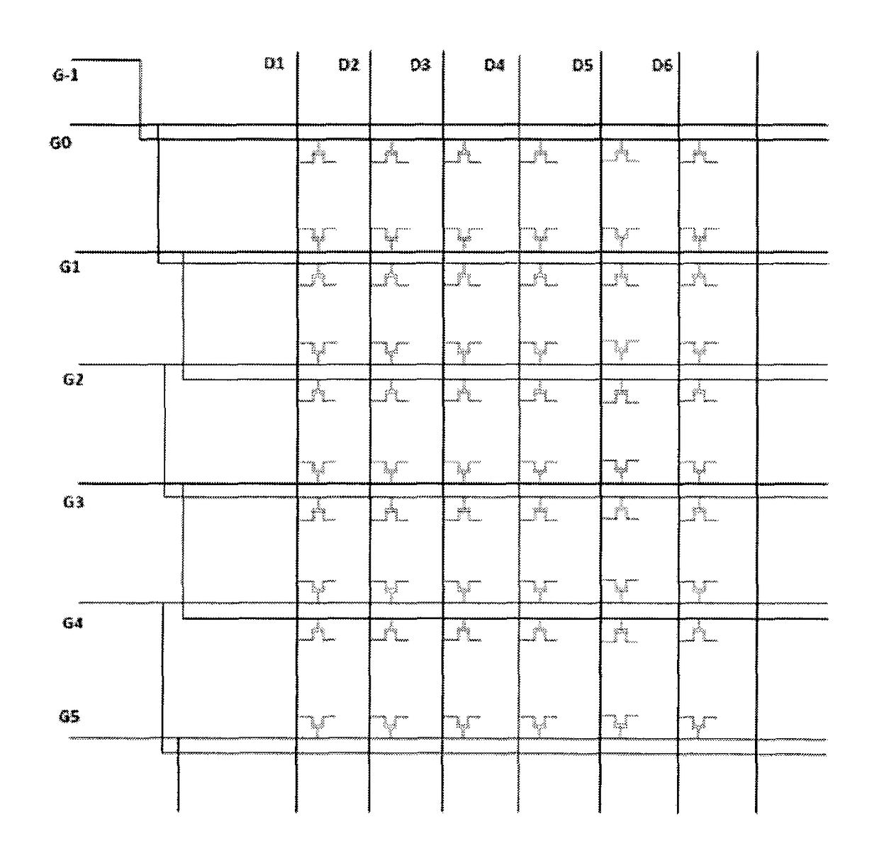
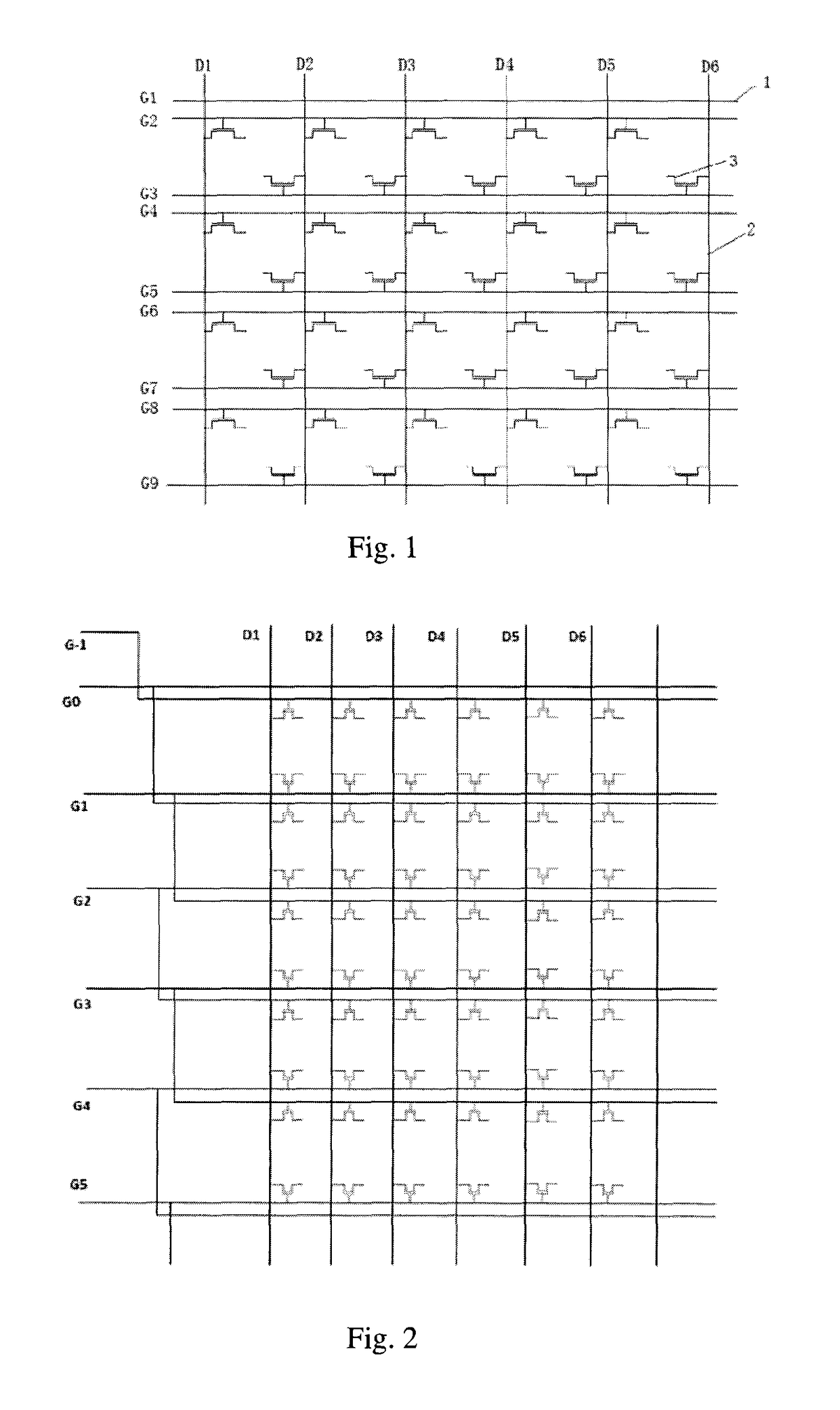
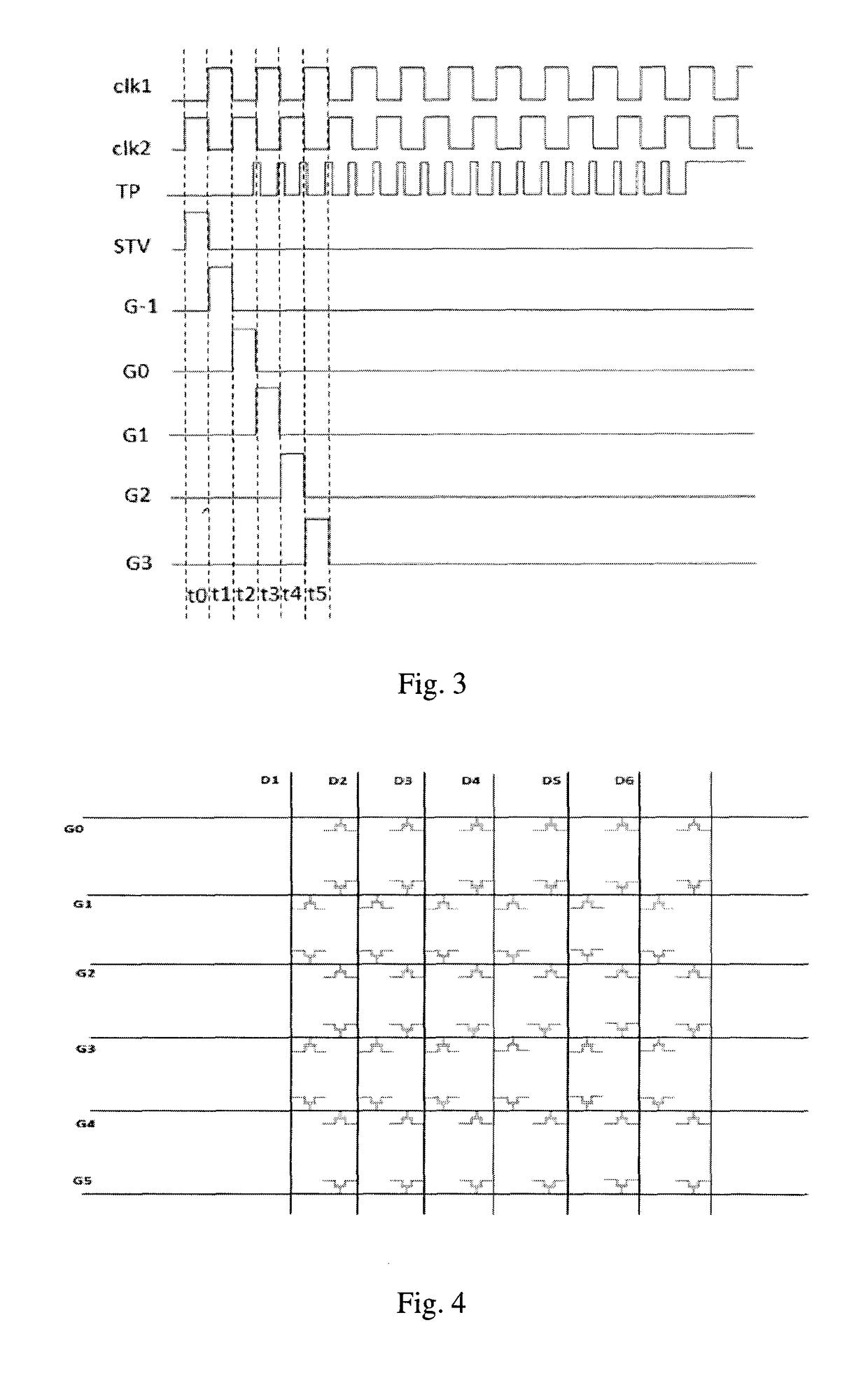
[0036]FIG. 1 schematically shows an existing array substrate which uses two TFTs to charge the same pixel electrode. As shown in FIG. 1, the array substrate comprises a plurality of scan lines arranged in parallel and a plurality of data lines arranged in a direction perpendicular the scan lines, among which D1 to D6 are data lines and ...


PUM

PropertyMeasurementUnit
gray scale voltageaaaaaaaaaa
voltageaaaaaaaaaa
electric fieldaaaaaaaaaa

Abstract

An array substrate includes a plurality of scan lines formed on a substrate in parallel, a plurality of data lines, which are formed on the substrate in a direction perpendicular to the respective scan lines, but disposed in a different layer from the scan lines, a plurality of pixel units respectively disposed in areas formed by the scan lines and the data lines, each pixel unit including at least one pixel electrode and at least two TFT switches. A first TFT switch pre-charges the pixel electrode, and a second TFT switch pre-charges the pixel electrode with gray scale voltage. A scan signal of at least one scan line enables the first TFT switches of the pixel units on in a line, and at the same time enables the second TFT switches of the pixel units on in another line. A method for driving the array substrate is also described.

Description

CROSS REFERENCE TO RELATED APPLICATION[0001]The present application claims benefit of Chinese patent application CN 201410397924.X, entitled “Array Substrate and Method for Driving the Same” and filed on Aug. 13, 2014, which is incorporated herein by reference.TECHNICAL FIELD[0002]The present disclosure relates to the technical field of display, and in particular, to an array substrate and a method for driving the array substrate.TECHNICAL BACKGROUND[0003]Due to the limitation of the manufacturing technology, impurities would mix in the liquid crystal molecules. The impurities will be ionized by the direct-current electric field and form polarization residual electric field. Under the action of the polarization residual electric field, even if no voltage is applied, the liquid crystal molecules would also deflect and develop certain light transmission effect. As a result, normal display of the liquid crystal panel is influenced.[0004]In order to eliminate the polarization residual e...

Claims


Application Information

Patent Timeline
Patent Type & Authority Patents(United States)
IPC IPC(8): G09G5/10G02F1/1362G09G3/36G02F1/1368
CPCG09G3/3659G02F1/1368G02F1/136286G02F1/13624G02F2201/123G09G3/3614G09G2300/0426G09G2310/08
Inventor XU, XIANGYANG
Owner TCL CHINA STAR OPTOELECTRONICS TECH CO LTD
Why Eureka
Try Eureka