Chuck table

a chuck table and chuck technology, applied in the field of chuck tables, can solve the problems of negative pressure leakage and the inability of the chuck table to fully attract the semiconductor wafer under suction, and achieve the effect of sufficient protection

Active Publication Date: 2018-10-02
DISCO CORP
View PDF21 Cites 2 Cited by
  • Summary
  • Abstract
  • Description
  • Claims
  • Application Information

AI Technical Summary

Benefits of technology

[0008]It is therefore an object of the present invention to provide a chuck table which is capable of preventing a negative pressure leakage from occurring and reliably holding a semiconductor wafer under suction when the front side of the semiconductor wafer on which a plurality of electrode bumps are formed is to be attracted under suction to the chuck table.

Problems solved by technology

When the front side of the semiconductor wafer is to be held under suction on the chuck table, the electrode bumps that protrude on the semiconductor devices are liable to cause a negative pressure leakage and the chuck table fails to exert a sufficient negative pressure on the semiconductor wafer.
Consequently, there is a problem that the chuck table is unable to fully attract the semiconductor wafer under suction.

Method used


Image

  • Chuck table
  • Chuck table
  • Chuck table

Examples


Embodiment Construction

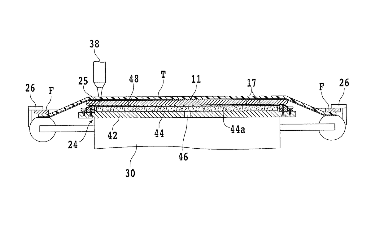
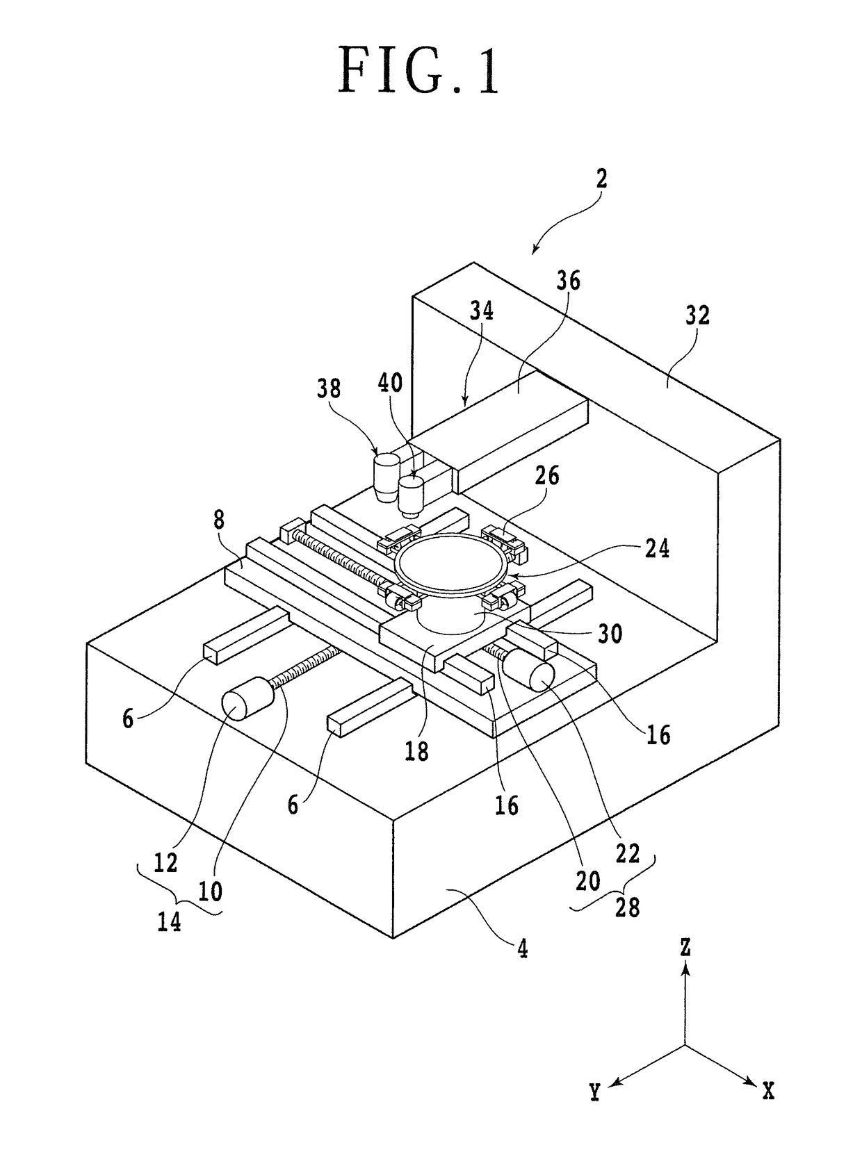
[0019]An embodiment of the present invention will be described in detail below with reference to the drawings. FIG. 1 schematically depicts in perspective a laser processing apparatus 2 incorporating a chuck table according to an embodiment of the present invention. The laser processing apparatus 2 includes a pair of guide rails 6 mounted on a stationary base 4 and extending in Y-axis directions. A Y-axis movable block 8 is slidably mounted on the guide rails 6. The Y-axis movable block 8 is moved along the guide rails 6 in indexing feed directions, i.e., the Y-axis directions, by a Y-axis feed mechanism (Y-axis feed means) 14 which includes a ball screw 10 and a pulse motor 12. The Y-axis movable block 8 supports a pair of guide rails 16 fixedly mounted thereon which extend in X-axis directions.

[0020]An X-axis movable block 18 is slidably mounted on the guide rails 16. The X-axis movable block 18 is moved along the guide rails 16 in processing feed directions, i.e., the X-axis dire...


PUM


Abstract

A chuck table holds under suction a front side of a wafer which includes a device region including a plurality of devices, each having a plurality of electrode bumps, formed in a plurality of areas demarcated in a grid pattern, and an outer peripheral extra region surrounding the device region. The chuck table includes a holding surface for facing the electrode bumps and holding under suction the device region of the wafer, and an outer peripheral extra region support surrounding the holding surface and including an elastic member projecting beyond the holding surface for supporting the outer peripheral extra region of the wafer. The outer peripheral extra region support projects from the holding surface by a distance corresponding to the height of the electrode bumps.

Description

BACKGROUND OF THE INVENTION[0001]Field of the Invention[0002]The present invention relates to a chuck table for use in a processing apparatus such as a laser processing apparatus or the like.[0003]Description of the Related Art[0004]According to a processing method that has started to be used in recent years for semiconductor wafers and optical device wafers wherein a light-emitting layer is formed on an epitaxial substrate made of sapphire, SiC, GaN, or the like, a laser beam which has a wavelength permeable to a wafer to be processed is applied to the wafer while being focused at a point within the wafer, forming a modified layer in the wafer, and then external forces are applied to the wafer to divide the wafer into individual device chips, with the modified layer acting as a fracture starting point (see, for example, Japanese Patent No. 3408805).[0005]The above processing method is subject to the condition that anything (e.g., materials for forming various patterns that make up ...

Claims


Application Information

Patent Timeline
Patent Type & Authority Patents(United States)
IPC IPC(8): H01L21/67H01L21/683
CPCH01L21/67092H01L21/6838H01L21/68721H01L21/6835H01L21/68742H01L21/68714H01L21/68771H01L21/6836
Inventor TOGASHI, KEN
Owner DISCO CORP
Why Eureka
Try Eureka