

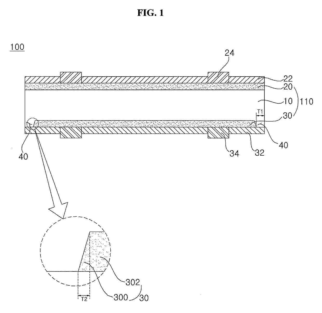
Solar cell and method for manufacturing the same
a solar cell and manufacturing method technology, applied in the field of solar cells, can solve the problems of efficient prevention of reverse current caused by connection of back electric field region to isolation portion, and achieve the effect of improving reliability and productivity and high efficiency
- Summary
- Abstract
- Description
- Claims
- Application Information
AI Technical Summary
Benefits of technology
Problems solved by technology
Method used
Image

Examples
example 1
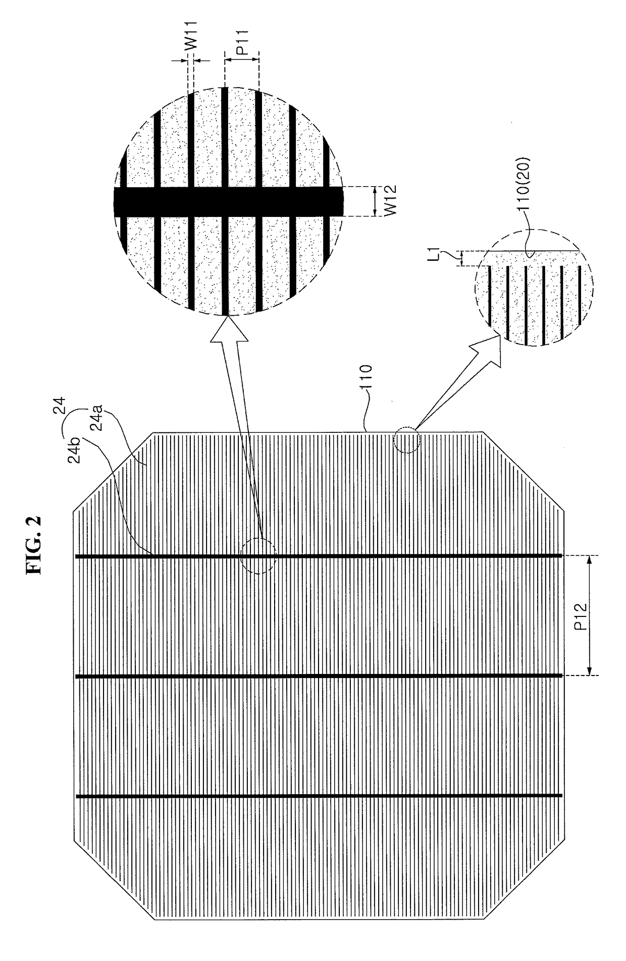
[0109]An n-type semiconductor substrate was prepared. A mask having a frame shape covering an edge of the semiconductor substrate was placed on a back surface of the semiconductor substrate and phosphorous (P) was ion-implanted to form a back electric field region and an isolation portion. At this time, a width of the portion of the mask covering the edge of the semiconductor substrate was 0.75 m (750 μm).
[0110]At a distance of 0 μm, 325 μm, 700 μm, 800 μm and 950 μm from the edge of the semiconductor substrate in Example 1, a doping concentration and a junction depth were calculated and / or measured. Results are shown in Table 1. In addition, the doping concentration is shown in a graph of FIG. 14 and the junction depth is shown in a graph of FIG. 15.
[0111]
TABLE 1Distance from edgeDoping concentrationJunction depth[μm][n / cm2][nm]06.56 × 1011653251.11 × 1014907.57002.61 × 101410398005.61 × 101520639505.85 × 10152172
[0112]As can be seen from Table 1 and FIGS. 14 and 15, at a distance ...
example 2
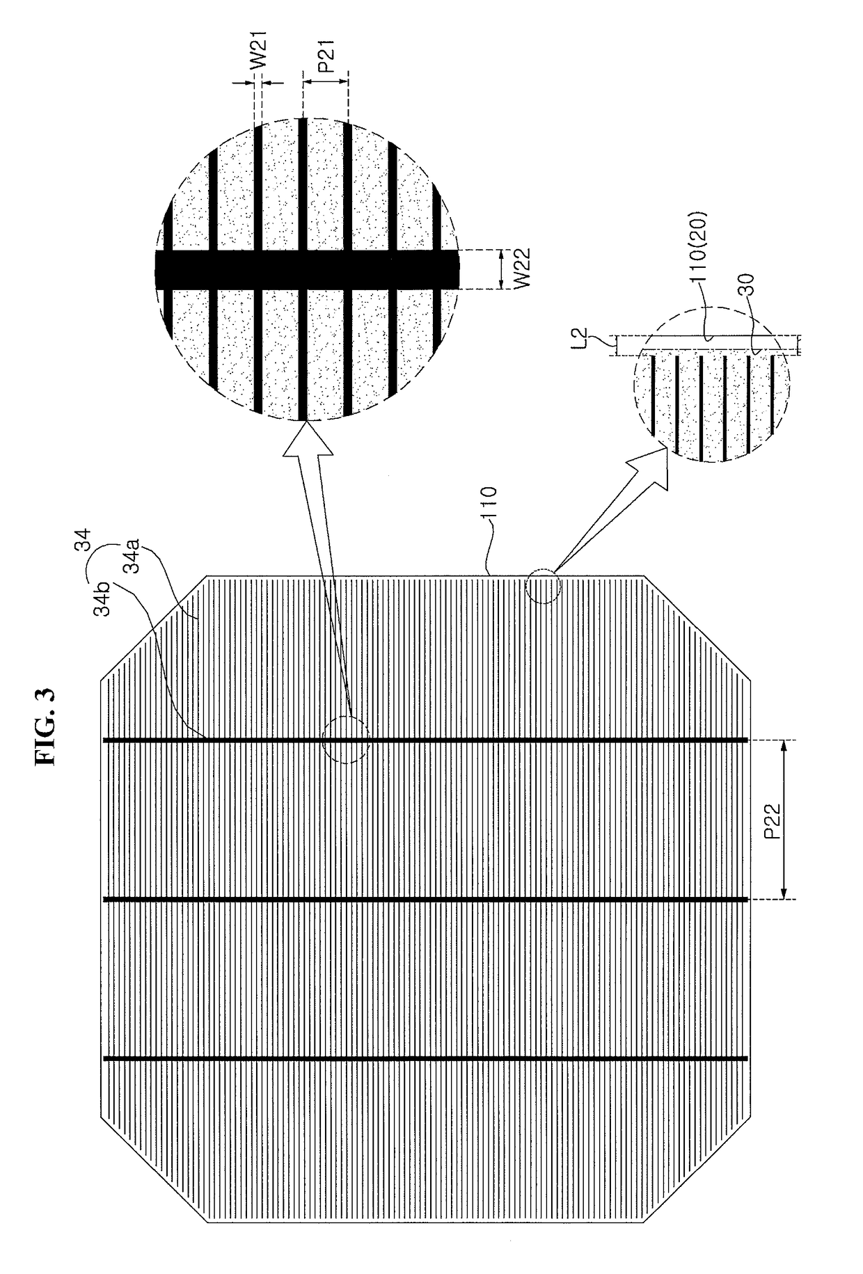
[0115]An n-type semiconductor substrate was prepared. A mask having a frame shape covering an edge of the semiconductor substrate was placed on a back surface of the semiconductor substrate and phosphorous (P) was ion-implanted to form a back electric field region and an isolation portion. At this time, a width of the portion of the mask covering the edge of the semiconductor substrate was 0.5 mm. In addition, boron (B) was ion-implanted on the front surface of the semiconductor substrate to form an emitter region. An anti-oxidation film and a first electrode were formed on the front surface of the semiconductor substrate, and a passivation film of the semiconductor substrate was formed to manufacture a solar cell.
example 3
[0116]A solar cell was manufactured in the same manner as in Example 2, except that the width of the portion of the mask covering the edge of the semiconductor substrate was 1.0 mm.
[0117]Reverse current (at −12V) of the solar cells manufactured in accordance with Examples 2 and 3 were measured and results are shown in Table 2.
[0118]
TABLE 2Reverse current [A]Example 20.62Example 31.74
[0119]As can be seen from Table 2, the solar cells in accordance with Examples 2 and 3 have considerably low reverse currents.
[0120]Particular features, structures, or effects described in connection with the embodiment of the invention are included in at least one embodiment of the invention and not necessarily in all embodiments of the invention. Furthermore, the particular features, structures, or effects of any specific embodiment of the invention may be combined in any suitable manner with one or more other embodiments of the invention or may be changed by those skilled in the art to which the embod...
PUM
 Abstract
Description
Claims
Application Information