Display device and driving method thereof

a display device and driving method technology, applied in the direction of instruments, static indicating devices, etc., can solve the problems of increasing the correction period, difficult to perform external correction in parallel with the display operation of the display device, and unintentional changes of the display, so as to reduce adverse effects, suppress uneven display, and reduce adverse effects

Active Publication Date: 2019-01-01
SEMICON ENERGY LAB CO LTD
View PDF133 Cites 7 Cited by
  • Summary
  • Abstract
  • Description
  • Claims
  • Application Information

AI Technical Summary

Benefits of technology

[0014]An object of one embodiment of the present invention is to provide a display device or the like which can perform external correction in parallel with display operation. An object of one embodiment of the present invention is to provide a driving method of the display device or the like which can perform external correction in parallel with display operation. An object of one embodiment of the present invention is to provide a display device in which display unevenness is suppressed, and a driving method thereof. An object of one embodiment of the present invention is to provide a display device capable of high definition display, and a driving method thereof. An object of one embodiment of the present invention is to provide a semiconductor device which can reduce adverse effects due to variation in transistor characteristics, and a driving method thereof. An object of one embodiment of the present invention is to provide a semiconductor device which can reduce adverse effects due to variation in the threshold voltages of transistors, and a driving method thereof. An object of one embodiment of the present invention is to provide a semiconductor device which can reduce adverse effects due to variation in the motilities of transistors, and a driving method thereof.
[0030]According to one embodiment of the present invention, a display device or the like which can perform external correction in parallel with display operation, can be provided. According to one embodiment of the present invention, a driving method of the display device or the like which can perform external correction in parallel with display operation, can be provided. According to one embodiment of the present invention, a display device in which display unevenness is suppressed and a driving method thereof can be provided. According to one embodiment of the present invention, a display device capable of high definition display and a driving method thereof can be provided. According to one embodiment of the present invention, a semiconductor device which can reduce adverse effects due to variation in transistor characteristics and a driving method thereof can be provided. According to one embodiment of the present invention, a semiconductor device which can reduce adverse effects due to variation in the threshold voltages of transistors and a driving method thereof can be provided. According to one embodiment of the present invention, a semiconductor device which can reduce adverse effects due to variation in the mobility of transistors and a driving method thereof can be provided.

Problems solved by technology

Thus, when the external correction is performed while the display operation is performed, display changes unintentionally.
For this reason, it is difficult to perform the external correction in parallel with the display operation of a display device.
Furthermore, in the case where the external correction is performed in a period where the display operation of the display device is not performed, there has been a problem in that a period for the correction is increased because the correcting operation needs to be performed for a considerable number of pixels.

Method used


Image

  • Display device and driving method thereof
  • Display device and driving method thereof
  • Display device and driving method thereof

Examples


embodiment 1

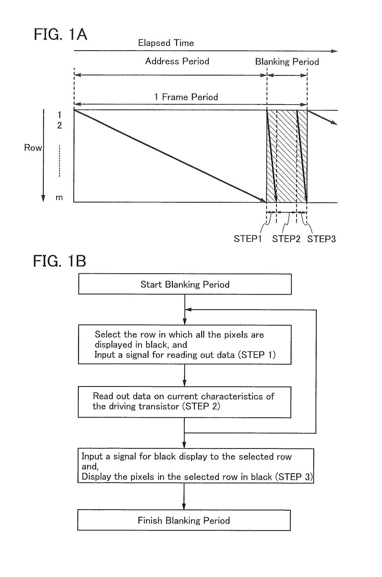
[0072]In this embodiment, a structure of a display device according to one embodiment of the disclosed invention and a driving method thereof will be described with reference to FIGS. 1A and 1B, FIG. 2, FIG. 3, FIG. 4, FIG. 5, FIG. 6, FIG. 7, FIGS. 8A and 8B, FIGS. 9A to 9C, FIG. 10, and FIGS. 11A and 11B.

[0073]FIG. 1A is a timing chart illustrating a driving method of a display device according to one embodiment of the disclosed invention. In the timing chart in FIG. 1A, the horizontal direction indicates elapsed time and the vertical direction indicates the row on which scanning is performed.

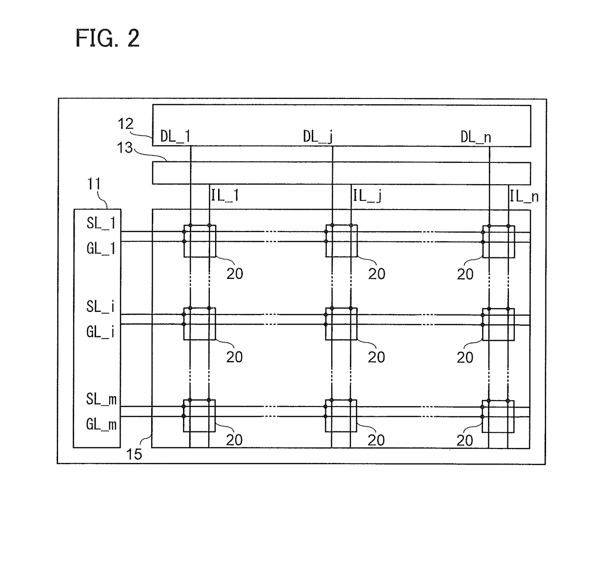
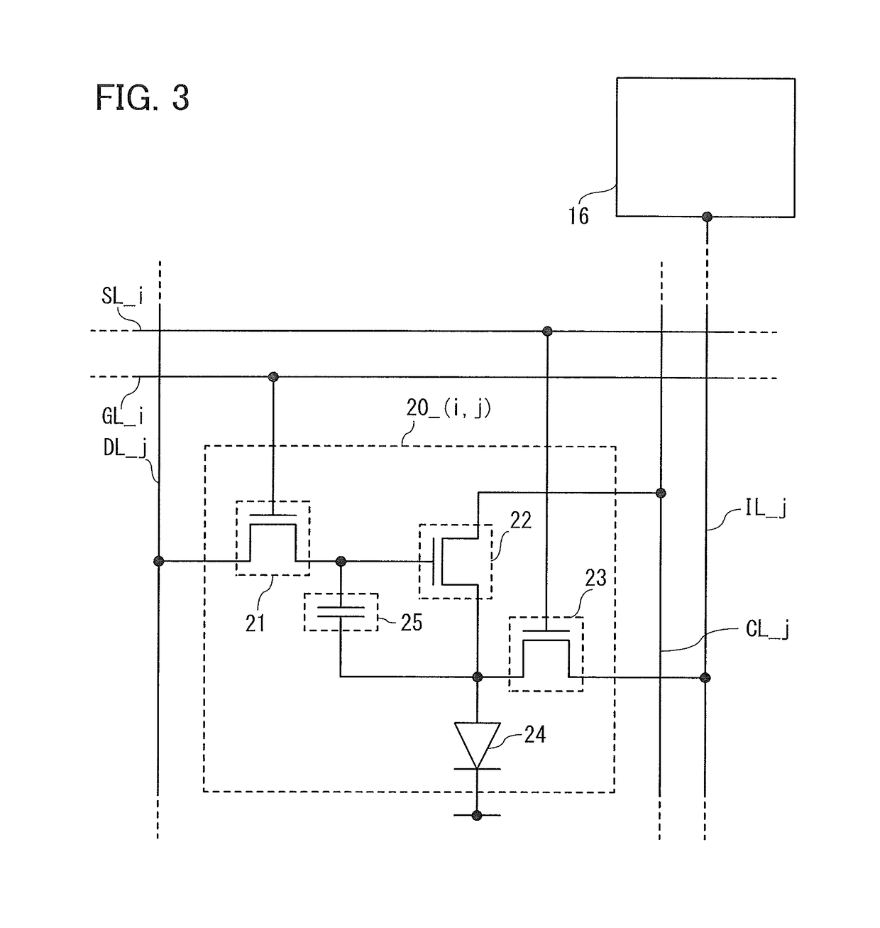
[0074]The display device of this embodiment includes a plurality of pixels arranged in a matrix with in rows and n columns (m and n are each an integer greater than or equal to 2). Furthermore, each pixel includes a light-emitting element and a transistor which supplies current to the light-emitting element (hereinafter also referred to as a driving transistor). Furthermore, the display device...

embodiment 2

[0177]In this embodiment, a structure of a display device and a driving method thereof which are different from those described in Embodiment 1 are described with reference to FIG. 12 and FIGS. 13A to 13C.

[0178]FIG. 12 shows a pixel structure of the display device of this embodiment. The display device of this embodiment includes, as in the display device in FIG. 2, the pixel portion 15 including (m×n) pixels 50, a variety of peripheral circuits, and a variety of wirings. The same numerals and symbols are used for the peripheral circuits and the wirings.

[0179]Because the pixel structure is different from that in Embodiment 1, the structures of the peripheral circuit and the wiring are partly different from those in FIG. 2. Specifically, the different points are that the wiring IL extends in the row direction and the circuit portion 13 is electrically connected to the wiring DL. In that case, as shown in FIG. 4, switches may be provided so that the circuit portion 13 and the driver c...

embodiment 3

[0229]In this embodiment, a structure of a display device and a driving method thereof which are different from those described in Embodiment 1 are described with reference to FIG. 16 and FIG. 17.

[0230]FIG. 16 shows a pixel structure of the display device of this embodiment. The display device of this embodiment includes, as in the display device in FIG. 2, the pixel portion 15 including (m×n) pixels 70, a variety of peripheral circuits, and a variety of wirings. The same numerals and symbols are used for the peripheral circuits and the wirings.

[0231]FIG. 16 shows a structure of a pixel 70_(i,j) in the i-th row and the j-th column (i is an integer greater than or equal to 1 and less than or equal to m and j is an integer greater than or equal to 1 and less than or equal to n). The pixel 70_(i, j) includes a transistor 71, a p-channel transistor 72, a transistor 73, a light-emitting element 74, and a capacitor 75. Note that these elements included in the pixel 70_(i,j) are electrical...


PUM


Abstract

To provide a display device which can perform external correction in parallel with display operation. The display device includes a plurality of pixels arranged in a matrix and a plurality of reading circuits provided outside the pixels. Each of the pixels includes a light-emitting element and a transistor which supplies current to the light-emitting element. In the display device, in a blanking period of the display device, a row in which all the pixels are displayed in black is selected so that a reading signal is input thereto; data on current characteristics of the transistors included in the pixels in the selected row is read out, and at the same time, display is performed in pixels in rows other than the selected row; and a signal for black display is input in the selected row so that the pixels in the row are displayed in black.

Description

BACKGROUND OF THE INVENTION[0001]1. Field of the Invention[0002]One embodiment of the present invention relates to a display device and a driving method of the display device.[0003]Note that one embodiment of the present invention is not limited to the above technical field. The technical field of the invention disclosed in this specification and the like relates to an object, a method, or a manufacturing method. In addition, one embodiment of the present invention relates to a process, a machine, manufacture, or a composition of matter. Specific examples of the technical field of one embodiment of the present invention disclosed in this specification include a semiconductor device, a display device, a light-emitting device, a power storage device, an imaging device, a memory device, a method for driving any of them, and a method for manufacturing any of them.[0004]2. Description of the Related Art[0005]In recent years, display devices have been used for various electronic devices s...

Claims


Application Information

Patent Timeline
Patent Type & Authority Patents(United States)
IPC IPC(8): G09G3/36G09G3/3291G09G3/3233
CPCG09G3/3291G09G3/3233G09G2300/0842G09G2320/045G09G2320/029G09G2320/0233G09G2320/0238G09G2310/0297
Inventor KIMURA, HAJIMEMIYAKE, HIROYUKI
Owner SEMICON ENERGY LAB CO LTD
Why Eureka
Try Eureka