Touch screen, touch panel, display device and electronic apparatus

a display device and touch screen technology, applied in the direction of cross-talk/noise/interference reduction, instruments, dielectric characteristics, etc., can solve the problems of extra parasitic capacitance formation, long life of touch panel, errors in detecting physical quantities, etc., and achieve the effect of reducing capacitance variations

Active Publication Date: 2019-02-19
TRIVALE TECH LLC
View PDF18 Cites 6 Cited by
  • Summary
  • Abstract
  • Description
  • Claims
  • Application Information

AI Technical Summary

Benefits of technology

[0013]The present invention has been made in view of the aforementioned problem and aims at providing a technique capable of reducing capacitance variations.
[0015]Since there is provided the larger interval between the outermost lead wiring and the first shield wiring, it is possible to reduce the capacitance variation.

Problems solved by technology

Further, such touch panels have longer lifetimes, because they have no movable portion which mechanically deforms.
However, in structures having a touch panel combined with a display element such as a liquid crystal display panel, an extra parasitic capacitance is formed between an outer lead wiring in the touch screen and the display element such as a liquid crystal display panel.
This causes errors in detecting physical quantities.

Method used


Image

  • Touch screen, touch panel, display device and electronic apparatus
  • Touch screen, touch panel, display device and electronic apparatus
  • Touch screen, touch panel, display device and electronic apparatus

Examples


first preferred embodiment

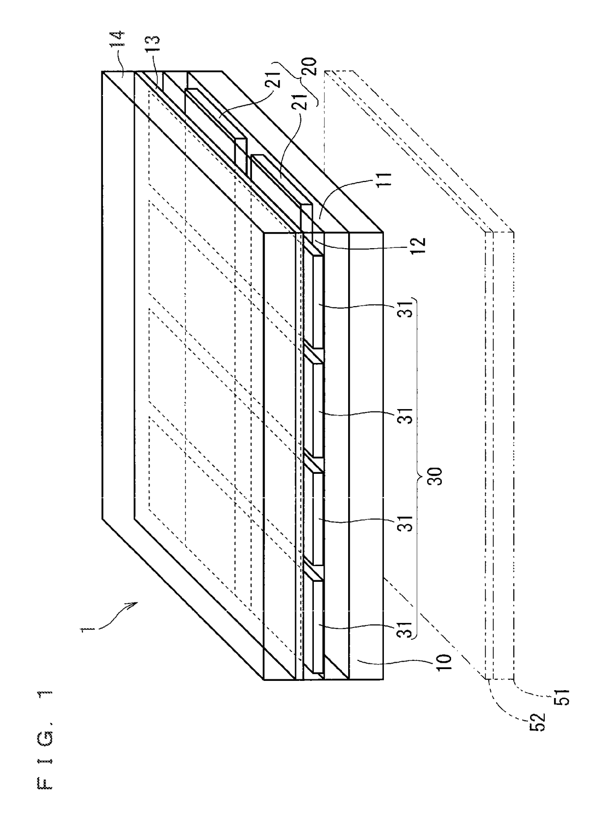
[0031]At first, with reference to FIGS. 1 to 8, there will be described a touch screen 1 according to a first preferred embodiment of the present invention. Note that the touch screen 1 according to the present first preferred embodiment will be described as being a projected-capacitive type touch screen, but is not limited thereto.

[0032]FIG. 1 is a perspective view illustrating the layer configuration in the touch screen 1 according to the present first preferred embodiment. Referring to FIG. 1, the touch screen 1 has a lowermost surface layer which is constituted by a transparent substrate 10 formed from a transparent glass material or a transparent resin. A lower electrode 20 is disposed on the transparent substrate 10. Further, an inter-layer insulation film 11 is disposed in such a way as to cover the lower electrode 20. The inter-layer insulation film 11 is a transparent insulation film such as a silicon nitride film or a silicon oxide film. An upper electrode 30 is disposed o...

second preferred embodiment

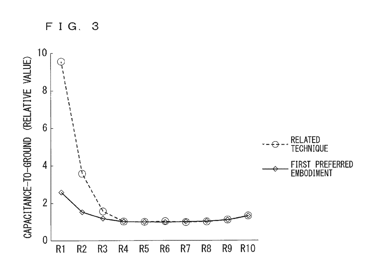
[0075]A second preferred embodiment of the present invention defines the bonding position of the adhesive member 52 (FIG. 1) for bonding the display element 51 to the touch screen 1 according to the first preferred embodiment, which can reduce the capacitances-to-ground of the lead wirings, and further reduce the capacitance variation. Note that the structure of the touch screen 1 is the same as that described with reference to FIGS. 1 to 8 in the first preferred embodiment.

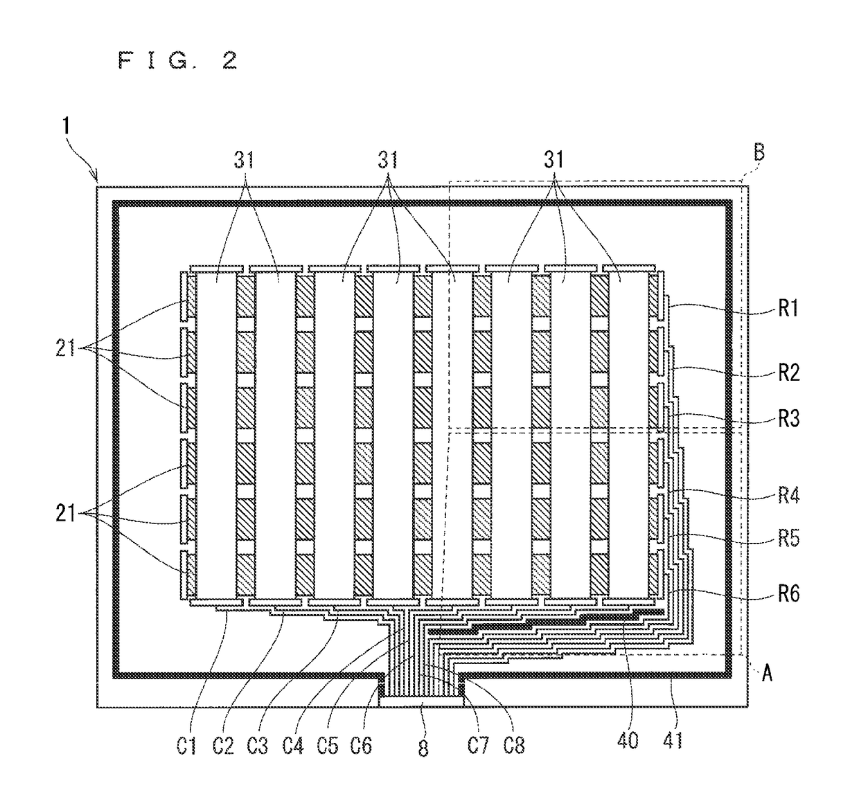
[0076]FIG. 9 is a plan view illustrating the structure of the touch screen 1 according to the present second preferred embodiment. The lead wirings R1 to R6 and C1 to C8, the column-direction wirings 21 and the row-direction wirings 31 are the same as those in the first preferred embodiment and, therefore, will not be described.

[0077]In FIG. 9, an imaginary line (two-dot chain line) indicates the outer contour line of the adhesive member 52 which bonds the touch screen 1 and the display element 51 to each other. ...

third preferred embodiment

[0081]A third preferred embodiment of the present invention defines the bonding position of the adhesive member 13 (FIG. 1) for bonding the transparent substrate 14 to the polarization plate which is not illustrated (which is substantially the transparent substrate 10), which can reduce the capacitance-to-ground of the outermost lead wiring R1, and further reduce the capacitance variation. Note that the structure of the touch screen 1 is the same as that described with reference to FIGS. 1 to 8 in the first preferred embodiment.

[0082]FIG. 11 is a plan view illustrating the structure of the touch screen 1 according to the present third preferred embodiment. The lead wirings R1 to R6 and C1 to C8, the column-direction wirings 21 and the row-direction wirings 31 are the same as those in the first preferred embodiment and, therefore, will not be described.

[0083]In FIG. 11, an imaginary line (two-dot chain line) indicates the outer contour line of the adhesive member 13. As indicated by ...


PUM


Abstract

A touch screen includes a first shield wiring surrounding a plurality of sensor wirings and a plurality of lead wirings, and capacitors. The distance between the first shield wiring and the outermost lead wiring which is the outermost wiring, out of the plurality of lead wirings, is larger than the intervals between the plurality of lead wirings. The capacitors are constituted by first and second electrodes including extending portions which extend in the extending direction.

Description

BACKGROUND OF THE INVENTION[0001]Field of the Invention[0002]The present invention relates to a touch screen, a touch panel, a display device, and an electronic apparatus.[0003]Description of the Background Art[0004]Touch panels are devices for detecting touches by fingers and the like and for identifying positional coordinates of the touched positions. Attention has been focused on such touch panels as one type of excellent user interface means. Currently, touch panels of various types such as resistive-film types and capacitive types have been fabricated as products. In general, a touch panel includes a touch screen incorporating touch sensors, and a detection device for identifying coordinates of touched positions based on signals from the touch screen.[0005]As one type of capacitive-type touch panels, there have been projected-capacitive type touch panels (refer to Japanese Patent Application Laid-Open No. 2012-103761, for example). Such a projected-capacitive type touch panel i...

Claims


Application Information

Patent Timeline
Patent Type & Authority Patents(United States)
IPC IPC(8): G06F3/041G06F3/044H05K1/02G06F1/16H05K1/16
CPCG06F3/0418G06F1/16G06F3/044H05K1/0219H05K1/162H05K2201/10128G06F2203/04107H05K2201/0108H05K2201/09354G06F3/0412G06F2203/04111G06F3/0445G06F3/0446
Inventor ONO, TAKESHINAKAMURA, TATSUYAMORI, SEIICHIRO
Owner TRIVALE TECH LLC
Why Eureka
Try Eureka