Capacitor structure

a capacitor and capacitor technology, applied in the structure of the radiating element, solid-state devices, basic electric elements, etc., can solve the problems of large capacitance value tolerances of this type of capacitors, large area consumed by capacitors, and poor accuracy of capacitance values, so as to reduce capacitance variation and improve the capacitance tolerance of the capacitor structure according to the invention

Pending Publication Date: 2022-05-05
COREHW SEMICON OY
View PDF5 Cites 0 Cited by
  • Summary
  • Abstract
  • Description
  • Claims
  • Application Information

AI Technical Summary

Benefits of technology

[0037]The present invention has the advantage that capacitance tolerance of the capacitor structure according to the invention is improved. In other words, capacitance values of capacitors with the invented capacitor structure are accurate without individual selection or trimming. The invented capacitor structure advantageously compensates effects of variation of layer thicknesses on the capacitance values due to manufacturing tolerances, thus reducing capacitance variation.

Problems solved by technology

Area consumed by capacitors is one major design restriction.
However, due to manufacturing process variations of this type of capacitor devices, capacitance value tolerances of this type of capacitors are large.
In other words, accuracy of the capacitance values is fairly poor, which causes challenges in manufacturing mass-produced devices for applications that require accurate capacitor values.
Individual selection of capacitors is not commercially feasible in mass production.
One known solution is to perform trimming of capacitors, which is somewhat more useful, but requires time and resources and thus adds cost.
Unfortunately, this kind of layer structure is not necessarily optimal layer structure in view of manufacturing tolerances, because the two thick metallization layers (L7, L9) will likely dominate in thickness variation, which contributes to increased capacitance variation.
These characteristics cause such vertical parallel plate capacitor type not to be suitable as such for example for antennas and / or antenna interfaces, in which accurate capacitor values are needed.
Ideally such compensation would cover all the used layers and all parts of the capacitor structure, but in a typical case, variation of all layers cannot be included in the compensation scheme.
For example, there may be limitations in the manufacturing process used for generating the capacitor structure.
However, even partial compensation reduces capacitance variation.

Method used


Image

  • Capacitor structure
  • Capacitor structure
  • Capacitor structure

Examples


Embodiment Construction

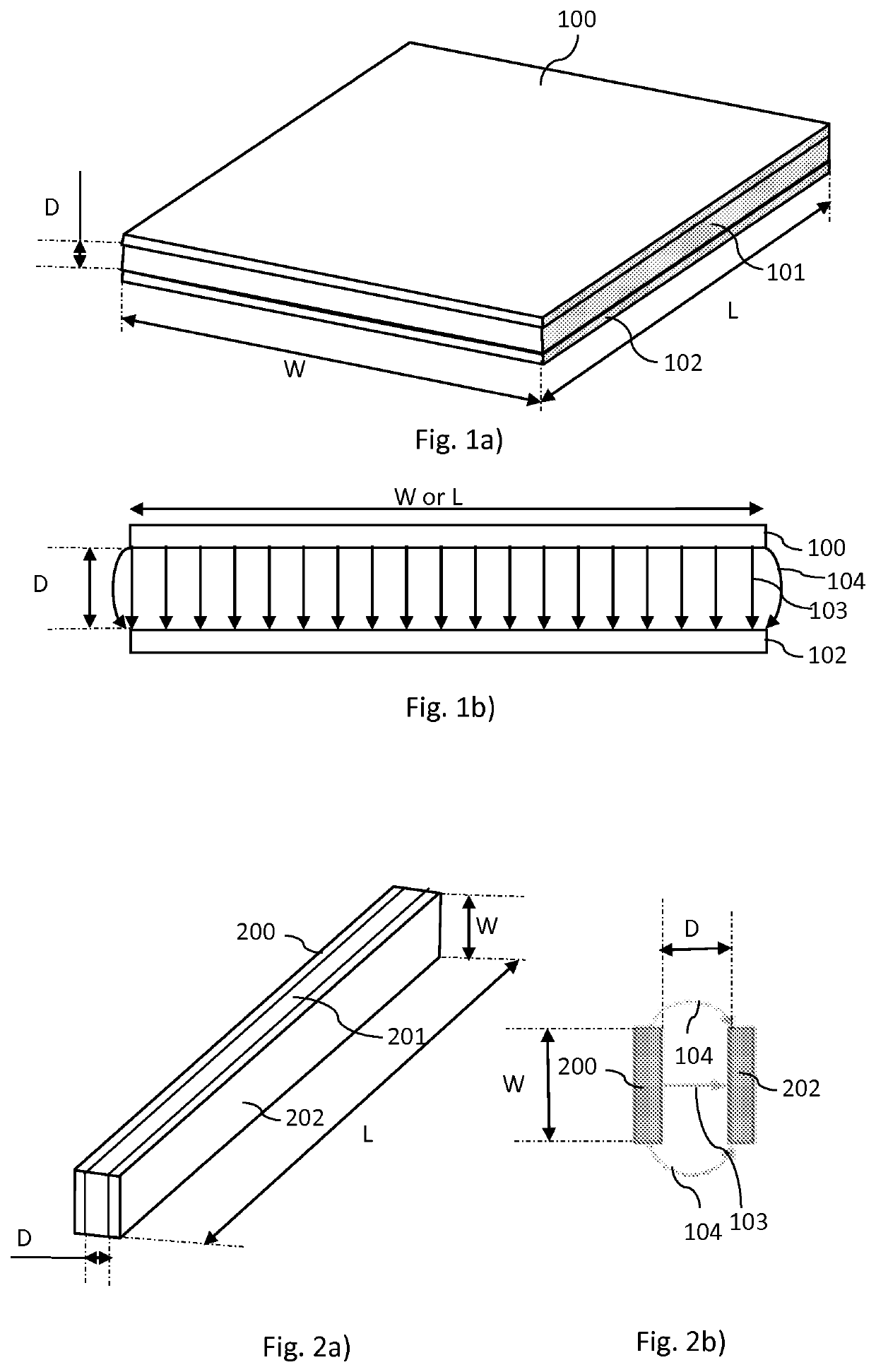
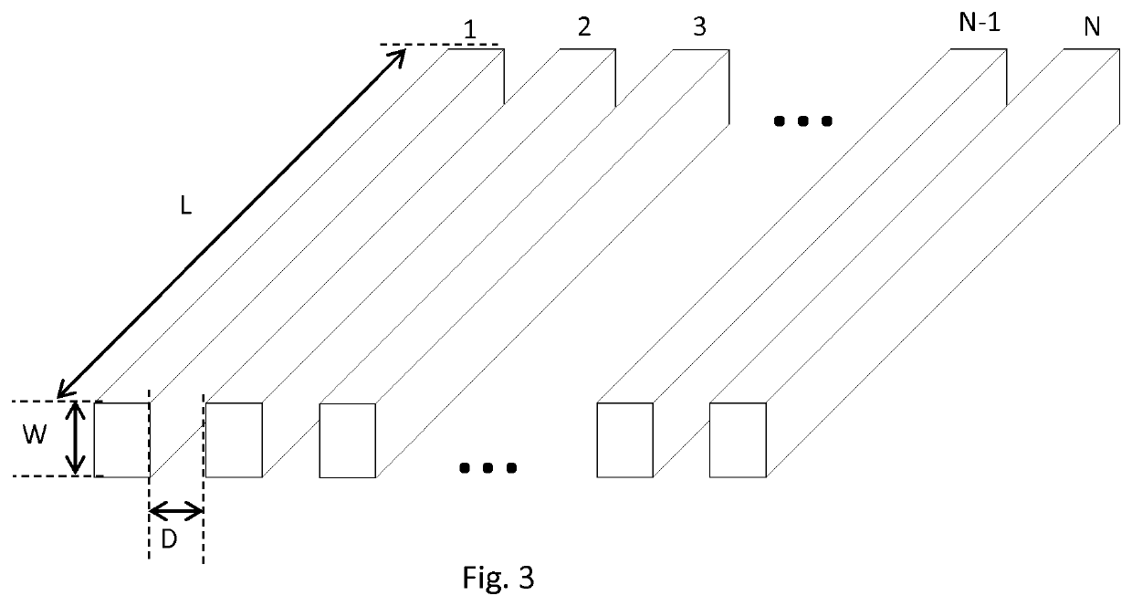
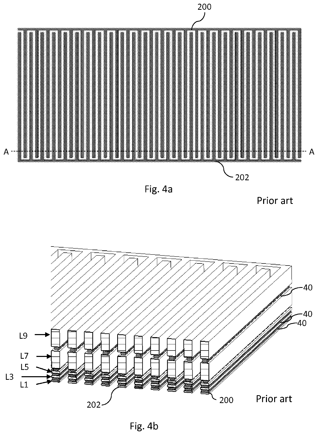
[0052]Terms variation and change refer to a situation in which a value of a physical quantity is different from its nominal value. For example, variation or change of a thickness of a layer due to manufacturing tolerances means that thickness of the layer in a final product is different from the nominal value that was used in the design to achieve wanted characteristics of associated physical quantities. Likewise, variation or change of a capacitance value due to variation of thickness of layers means that the capacitance value is different from the nominal value that would be achieved, if all layers had their nominal thickness as used in designing the capacitor.

[0053]As known in the art, a metal-dielectric device is typically manufactured in layers. In a layered structure, both terms lateral and horizontal are commonly used to refer to a structure or a field, such as an electric field, that extends along a layer of material. A lateral structure may be arranged between other lateral...


PUM

PropertyMeasurementUnit
dielectricaaaaaaaaaa
thicknessaaaaaaaaaa
polaritiesaaaaaaaaaa

Abstract

A capacitor structure implemented as a layered structure including a plurality of alternating dielectric and metallization layers, and a method of manufacturing such capacitor structure. The capacitor structure including at least one lateral parallel plate capacitor part (LPP part) including two first electrodes on two different layers separated by dielectric material of a plurality of the alternating layers, and at least one vertical parallel plate capacitor part (VPP part) including two second electrodes each including a plurality of superimposed slabs or bars arranged on a plurality of the metallization layers. The at least one LPP part is electrically coupled with the at least one VPP part to form the capacitor structure. A variation in capacitance value of the at least one LPP part due to a variation of thickness of dielectric material is at least partially compensated by an opposite variation in capacitance value of the at least one VPP part.

Description

FIELD[0001]The present invention relates to a capacitor device structure and a method for manufacturing such structure.BACKGROUND[0002]FIG. 1a shows a parallel plate capacitor with two laterally oriented conductor plates having a conductor plate length L, conductor plate width W and vertical distance between two plate electrodes (100, 102) is D. A gap between the first plate electrode (100) and the second plate electrode (102) is filled with dielectric medium (101) having thickness D and relative permittivity of ϵr and ϵ0 is constant for permittivity of vacuum. Capacitance of the parallel plate capacitor is given by equation:C=ϵ0×ϵr×(W×L) / D  (1)[0003]In semiconductor industry, when insulator is used as the dielectric medium (101), this kind of capacitor is commonly manufactured by placing one or more layers of insulator material between two flat sheets of metal, and thus it is commonly called as a Metal-Insulator-Metal (MIM) capacitor. This type of capacitor may be referred to as a ...

Claims


Application Information

Patent Timeline
Patent Type & Authority Applications(United States)
IPC IPC(8): H01L49/02
CPCH01L28/88H01L28/91H01L28/40H01L23/5223H01L28/86H01L28/90H01L23/5226H01L23/66H01L2223/6677H01Q1/2283H01Q1/38
Inventor HAKAMO, MARKUSTAKALO, TOMI-PEKKAKOTILAINEN, PETRIHELIÖ, PETRIKUIRI, TAPIO
Owner COREHW SEMICON OY
Why Eureka
Try Eureka