Variable capacitance element, packaged circuit, resonant circuit, communication apparatus, communication system, wireless charging system, power supply apparatus, and electronic apparatus

a technology of capacitance element and variable capacitor, which is applied in the direction of variable capacitor, inductance, transportation and packaging, etc., can solve the problem of wide variation in capacitance among variable capacitors, and achieve the effect of reducing capacitance variation

Active Publication Date: 2019-02-05
DEXERIALS CORP
View PDF11 Cites 0 Cited by
  • Summary
  • Abstract
  • Description
  • Claims
  • Application Information

AI Technical Summary

Benefits of technology

[0023]As mentioned above, the variable capacitance element according to the present disclosure allows the capacitance of the variable capacitance element to be adjusted after the variable capacitance element is mounted on an external circuit board or the like. Therefore, the present disclosure enables a reduction in capacitance variation among the variable capacitance elements.

Problems solved by technology

Thus, due to a manufacturing error and the like, a wider variation in capacitance among variable-capacitance capacitors is caused.

Method used


Image

  • Variable capacitance element, packaged circuit, resonant circuit, communication apparatus, communication system, wireless charging system, power supply apparatus, and electronic apparatus
  • Variable capacitance element, packaged circuit, resonant circuit, communication apparatus, communication system, wireless charging system, power supply apparatus, and electronic apparatus
  • Variable capacitance element, packaged circuit, resonant circuit, communication apparatus, communication system, wireless charging system, power supply apparatus, and electronic apparatus

Examples


modified example 1

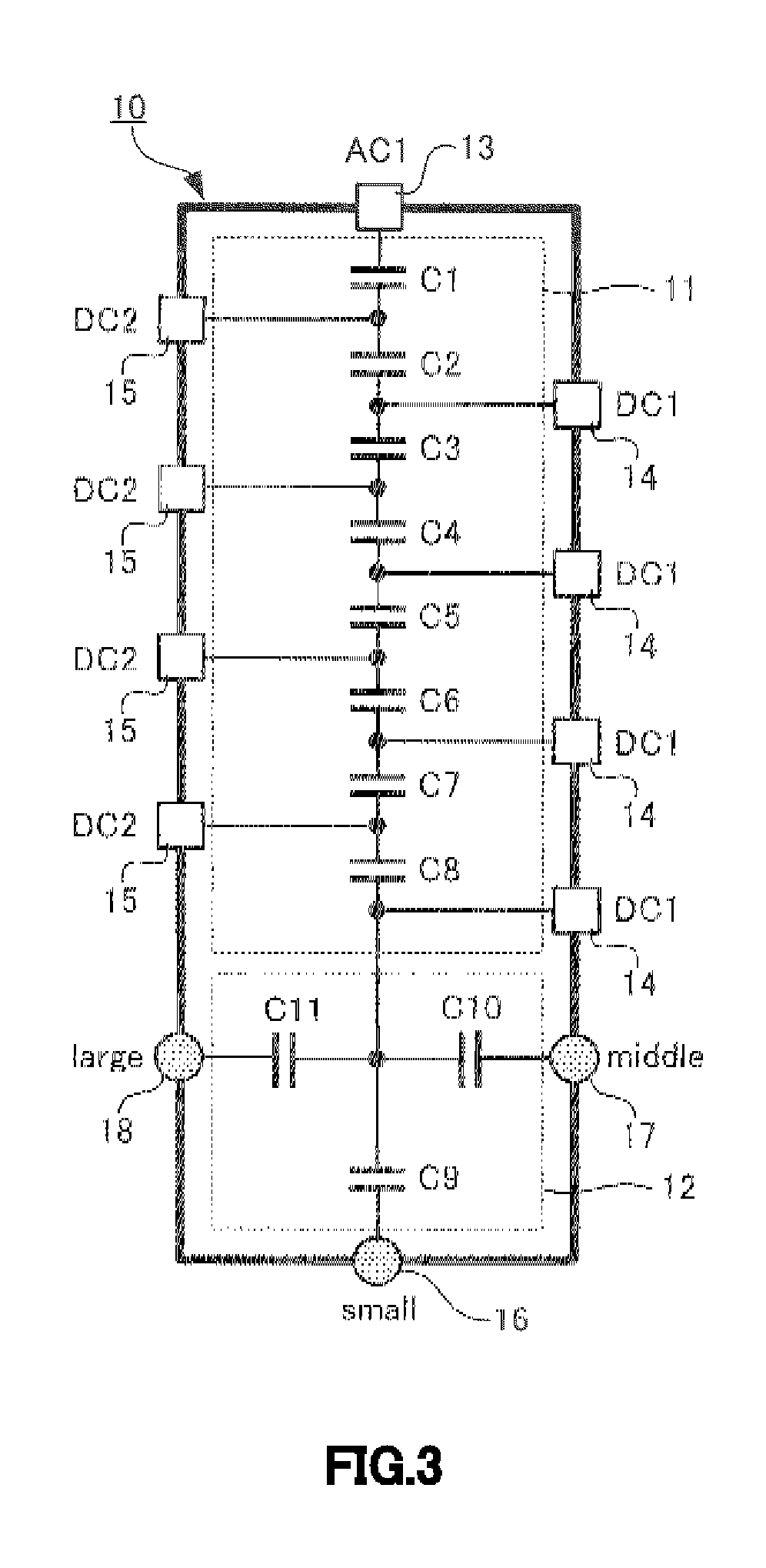
[0125]In the above-mentioned first embodiment, there was described an example in which, when the variable capacitance element 10 is mounted on the packaged circuit 20, the first external terminals for compensation 16 to the third external terminals for compensation 18 are connected to each other via the external wiring 21 (a large-capacitance connection state), but, the present disclosure is not limited to this embodiment. There may be employed a configuration of a packaged circuit, the configuration being such that, when the variable capacitance element 10 is mounted on the packaged circuit, the first external terminal for compensation 16 to the third external terminal for compensation 18 are not connected to each other via the external wiring 21. In Modified Example 1, an example of such configuration will be described.

[0126](1) Configuration of Packaged Circuit

[0127]FIG. 7 illustrates a schematic configuration of a packaged circuit of Modified Example 1 in which the variable capa...

modified example 2

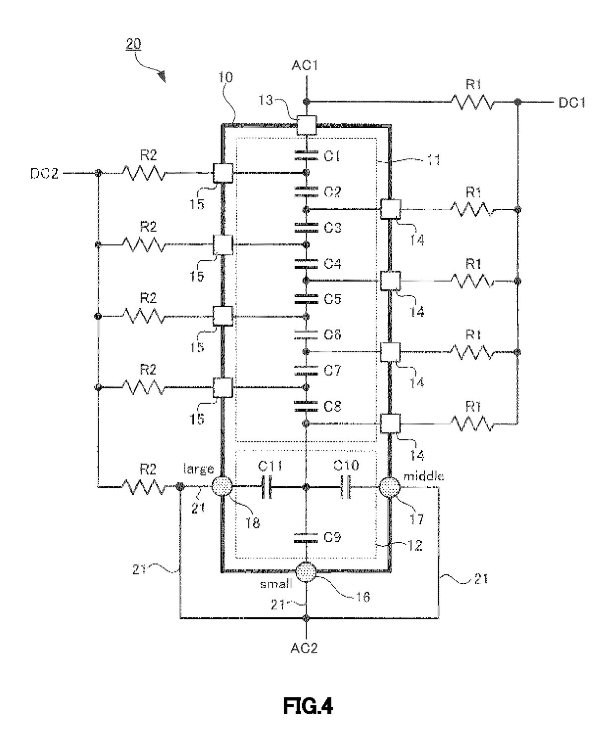
[0142]There were described the examples in which, in the above-mentioned first compensation (FIG. 5) and second compensation (FIG. 8) for capacitance variation of the variable capacitance element 10, a connection state of the compensation unit 12 was changed to three states, namely, a large-capacitance, a middle-capacitance, and a small-capacitance connection state. That is, in the above-mentioned first compensation and second compensation, the capacitance of the variable capacitance element 10 was changed in three steps. However, the present disclosure is not limited to this. According to a necessary range of capacitance variation of the variable capacitance element 10, a connection state of the compensation unit 12 may be changed between two connection states selected from a large-capacitance, a middle-capacitance, and a small-capacitance connection state (the capacitance of the variable capacitance element 10 is changed in two steps) thereby to compensate a capacitance variation....

modified example 3

[0199]In the above-mentioned second embodiment, there was described an example in which a capacitance variation is compensated by cutting the pattern of the external wiring 21 connecting the external terminals for compensation, as is the case with the first compensation described in the above-mentioned first embodiment, but, the present disclosure is not limited to this embodiment. Also in the present embodiment, as is the case with the second and the third compensations described in the above-mentioned Modified Examples 1 and 2, respectively, capacitance variation may be compensated by a pattern connection of the external wiring 21.

[0200]In this case, a packaged circuit is configured such that, when the variable capacitance element 30 is mounted on the packaged circuit, the wiring pattern of the external wiring 21 between the first external terminal for compensation 16 and the second external terminal for compensation 17 is the same as a wiring pattern illustrated in FIG. 15. In ot...


PUM

PropertyMeasurementUnit
resistanceaaaaaaaaaa
frequencyaaaaaaaaaa
carrier frequencyaaaaaaaaaa

Abstract

The present provides a variable capacitance element enabling a further reduction in capacitance variation among variable capacitance elements, and provides a packaged circuit including the variable capacitance element. A variable capacitance element is configured to include an element body unit, a compensation unit, a first external terminal for signals, a second external terminal for signals, external terminals for control, and external terminals for capacitance compensation. The compensation unit has second variable-capacitance capacitor units C9 to C 11, each including a second dielectric layer formed of a ferroelectric material, and is connected to the element body unit, and has a capacitance varying according to a control voltage signal.

Description

FIELD OF THE INVENTION[0001]The present application asserts priority rights based on JP Patent Application 2012-176665 filed in Japan on Aug. 9, 2012. The total contents of disclosure of the patent application of the senior filing date are to be incorporated by reference into the present application.[0002]The present disclosure relates to a variable capacitance element having a capacitance which varies by the application of a control voltage; a packaged circuit including the variable capacitance element; a resonant circuit; a communication apparatus; a communication system; a wireless charging system; a power supply apparatus; and an electronic apparatus.BACKGROUND OF THE INVENTION[0003]Conventionally, as a variable-capacitance capacitor applicable to a system and an apparatus (electronic apparatus) each requiring a capacitance adjustment, a variable-capacitance capacitor made of a ferroelectric material has been proposed. Such variable-capacitance capacitor has a high relative diel...

Claims


Application Information

Patent Timeline
Patent Type & Authority Patents(United States)
IPC IPC(8): H01G7/00H02J50/12H02J5/00H02J7/02H01G7/06H01F38/14H02J7/00
CPCH01G7/00H01G7/06H02J50/12H02J7/025H02J5/005H02J7/007H02J7/00
Inventor KANNO, MASAYOSHISAITO, NORIO
Owner DEXERIALS CORP
Why Eureka
Try Eureka