Electro-optical device having a storage capacitor formed by a data line and a potential line

a technology of potential line and electronic device, which is applied in the direction of instruments, static indicating devices, etc., can solve the problems of deteriorating display quality and difficulty in output data signals with extremely fine precision, and achieve high precision, suppressing the generation of luminance unevenness, and high data signal. the effect of precision

Active Publication Date: 2018-05-29
SEIKO EPSON CORP
View PDF24 Cites 0 Cited by
  • Summary
  • Abstract
  • Description
  • Claims
  • Application Information

AI Technical Summary

Benefits of technology

[0009]An advantage of some aspects of the invention is that it provides an electro-optical device, and an electronic apparatus for which a highly precise data signal is not necessary, and which are capable of supplying current to a light-emitting element with high precision while suppressing the generation of luminance unevenness.
[0011]According to the aspect of the invention, the second storage capacitor is formed by data lines and potential lines which are adjacent to each other. Since the data lines and potential lines are provided from one end to the other end of a region provided with a plurality of pixel circuits, the second storage capacitor has a sufficiently large capacitance in comparison with the first storage capacitor provided in the pixel circuit. Further, variation in the capacitance of the second storage capacitors of each column depends on errors in the semiconductor processing; however, since the second storage capacitor is formed by electrodes having a large area such as the data lines and the potential lines, it is possible to reduce the relative variation of the capacitance of the second storage capacitor.
[0013]As described above, since the variation of the capacitance of each of the plurality of second storage capacitors provided corresponding to each of the plurality of data lines is small, it is also possible to suppress variation in each column of the voltage of the gate of the driving transistor to be small. Accordingly, the electro-optical device according to the aspect suppresses the generation of display unevenness and is capable of high quality display.
[0015]According to the aspect of the invention, the data signal of the potential regulating the luminance of the light-emitting element is supplied to one end of the third storage capacitor. The data lines are connected to the other end of the third storage capacitor and configure one end of the second storage capacitor. Accordingly, the range of potential fluctuations of the data lines becomes a value in which the range of potential fluctuations of the data signals is compressed according to the capacitance ratio of the third storage capacitor with respect to the second storage capacitor. Since the second storage capacitor formed by the data lines and the potential lines has a large capacitance, the range of potential fluctuations of the data lines can be compressed to be sufficiently small in comparison with the range of potential fluctuations of the data signals. In this manner, even without cutting up the data signals with fine precision, it is possible to supply the current with respect to the light-emitting element with good precision.
[0016]Further, since the variation of the capacitance of each of the plurality of second storage capacitors provided corresponding to the plurality of data lines as described above is small, it is also possible to suppress the variation in the compression rate of the potential fluctuations of the data lines with respect to the potential fluctuations of the data signals to be small, and a high quality display in which the generation of luminance unevenness is prevented is possible.
[0018]According to the aspect of the invention, it is possible to suppress the influence of the holding voltage of the capacitor having a parasitic effect upon the light-emitting element.

Problems solved by technology

In a circuit having such a high driving ability, it is difficult to output data signals with extremely fine precision.
Further, when the pixel circuit is miniaturized, luminance unevenness caused by errors generated during manufacturing is generated and this has led to deterioration in the display quality in some cases.

Method used


Image

  • Electro-optical device having a storage capacitor formed by a data line and a potential line
  • Electro-optical device having a storage capacitor formed by a data line and a potential line
  • Electro-optical device having a storage capacitor formed by a data line and a potential line

Examples


first embodiment

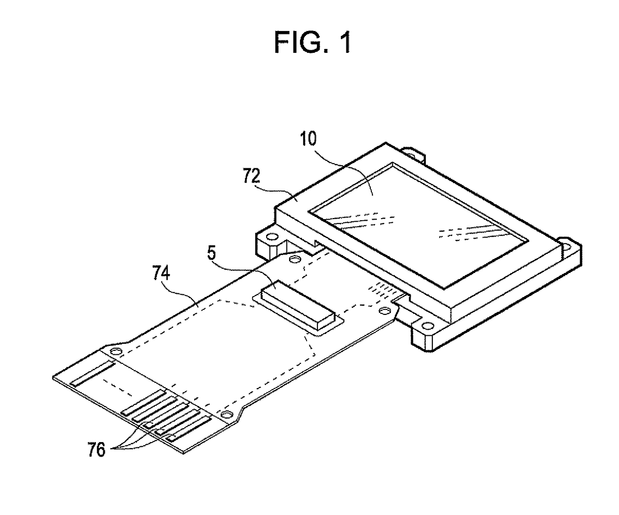
[0049]FIG. 1 is a perspective view showing a configuration of an electro-optical device 10 according to an embodiment of the invention.

[0050]For example, the electro-optical device 10 is a micro display displaying an image in a head mounted display. Detailed description will be given of the electro-optical device 10 later; however, the device is an organic EL apparatus in which a plurality of pixel circuits and driving circuits or the like driving the pixel circuits are formed on a silicon substrate, for example, in which an OLED which is an example of a light-emitting element is used in the pixel circuits.

[0051]The electro-optical device 10 is accommodated in an opening in a display unit or a see-through frame-shaped case 72, and one end of an FPC (Flexible Printed Circuit) substrate 74 is connected thereto. In the FPC substrate 74, a control circuit 5 of a semiconductor chip is mounted using a COF (Chip On Film) technique and a plurality of terminals 76 are provided and connected ...

second embodiment

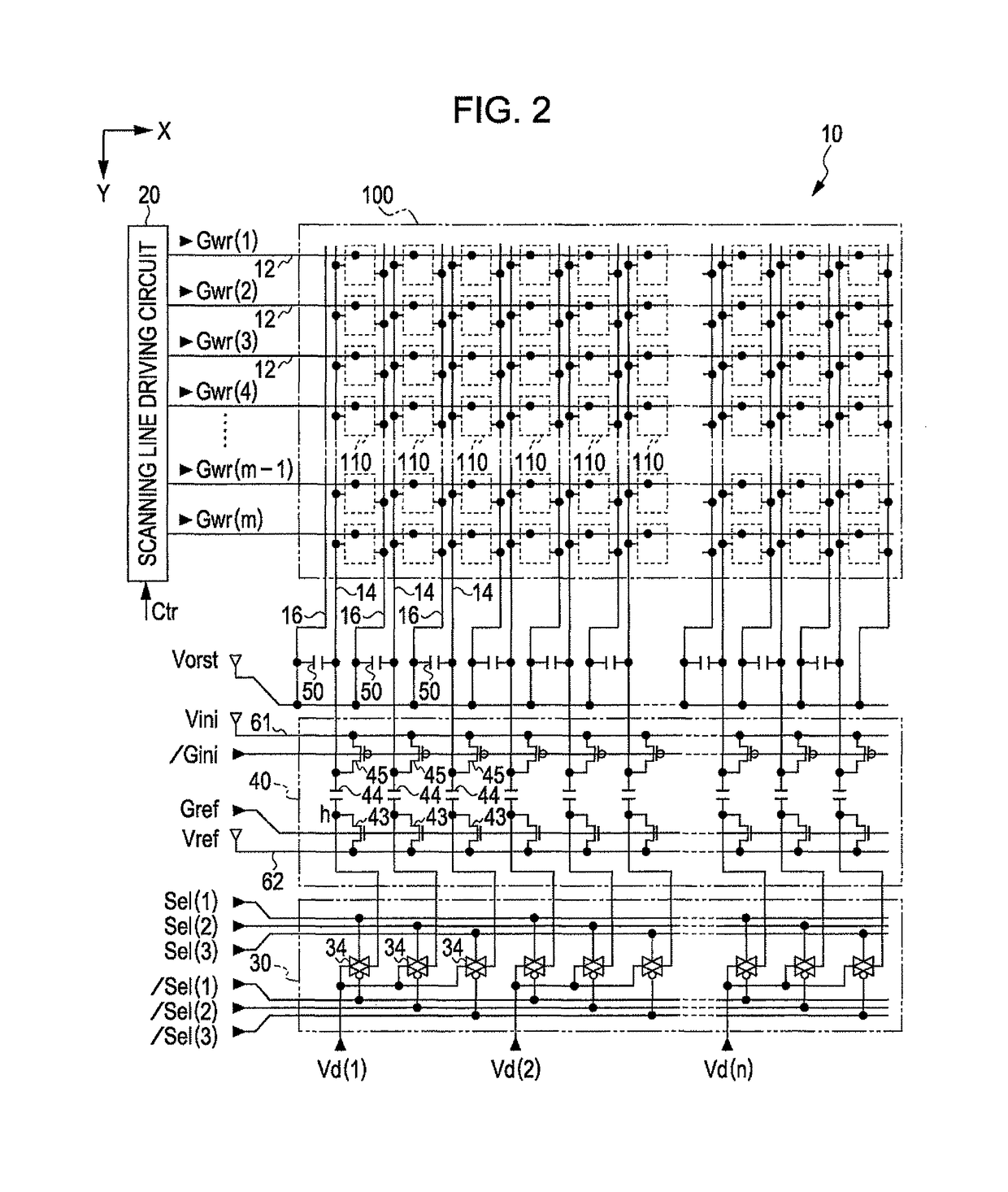
[0186]In the first embodiment, a configuration is adopted in which data signals are directly supplied by the demultiplexer 30 to the other ends of the storage capacitors 44 of each column, that is, to the nodes h. For this reason, in the scanning period of each row, since the period in which the data signals are supplied by the control circuit 5 is equal to the writing period, the time constraints are large.

[0187]Here, description will be given of the second embodiment in which it is possible to relax such time constraints. Here, in the following, in order to avoid duplication of explanation, description will be given with a focus on the parts which are different to the first embodiment.

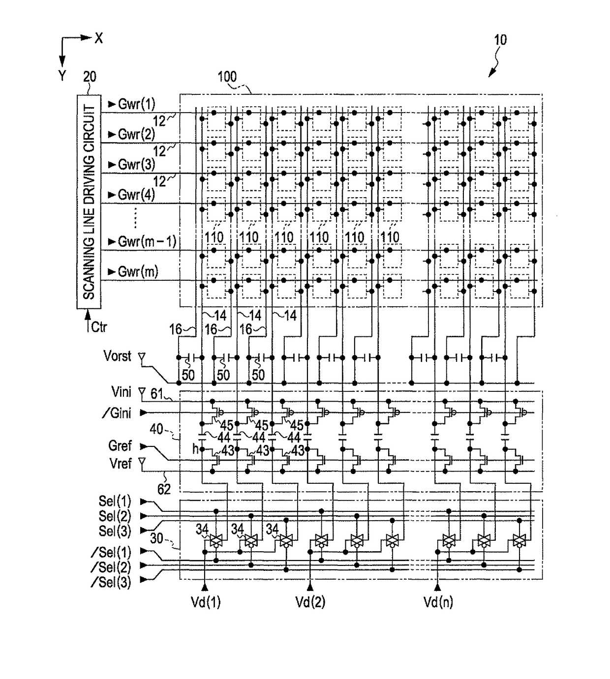
[0188]FIG. 13 is a view showing a configuration of an electro-optical device 10 according to the second embodiment.

[0189]The points where the second embodiment shown in the drawing is different to the first embodiment shown in FIG. 2 are mainly the points that a storage capacitor 41 and a transmissio...

application and modification examples

[0226]The invention is not limited to embodiments such as the above-described embodiments and application examples, and, for example, various modifications are possible as described in the following. Further, one or a plurality of arbitrarily selected forms of the modifications described below can also be combined as appropriate.

Control Circuit

[0227]In the embodiment described above, the control circuit 5 supplying data signals is set as separate to the electro-optical device 10; however, the control circuit 5 may also be integrated in the silicon substrate with the scanning line driving circuit 20, the demultiplexer 30 and the level shift circuit 40.

Substrate

[0228]In the above-described embodiments and modification examples, a configuration has been adopted in which the electro-optical device 10 is integrated in a silicon substrate; however, a configuration of integration with another semiconductor substrate may be adopted. Further, the device may be formed on a glass substrate or ...


PUM


Abstract

An electro-optical device is provided with a plurality of data lines, a plurality of potential lines supplied with a predetermined potential, a driving transistor controlling a current level according to the voltage between the gate and the source, a first storage capacitor which holds the voltage between the gate and a source of the driving transistor, and a light-emitting element. One data line among the plurality of data lines and one potential line among the plurality of potential lines are arranged to be adjacent to each other, and a second storage capacitor holding the potential of the one data line is formed by the one data line and the one potential line.

Description

BACKGROUND[0001]1. Technical Field[0002]The present invention relates to an electro-optical device and an electronic apparatus useful when a pixel circuit is miniaturized, for example.[0003]2. Related Art[0004]In recent years, various types of electro-optical devices using light-emitting elements such as organic light emitting diodes (below, “OLED”) have been proposed. In such electro-optical devices, pixel circuits including the above-described light-emitting elements, transistors, and the like corresponding to intersections of scanning lines and data lines are generally configured to be provided corresponding to the pixels of the image to be displayed. In such a configuration, when a data signal of a potential according to the gradation level of the pixels is applied to the gate of the transistor, the transistor supplies current according to the voltage between the gate and the source to the light-emitting element. In this manner, the light-emitting element emits light with a lumi...

Claims


Application Information

Patent Timeline
Patent Type & Authority Patents(United States)
IPC IPC(8): G09G3/3233G09G3/3291
CPCG09G3/3291G09G3/3233G09G2300/0814G09G2300/0838G09G2300/0861G09G2320/045G09G2310/0256G09G2310/0275G09G2310/0289G09G2310/0297G09G2300/0876
Inventor KASAI, TOSHIYUKINOMURA, TAKESHI
Owner SEIKO EPSON CORP
Why Eureka
Try Eureka