Supercharge Your Innovation With Domain-Expert AI Agents!

Electronic device

a near field communication and electronic device technology, applied in the structure of radiating elements, near-field systems using receivers, antenna earthings, etc., can solve the problems of etc., to save cost and space saving, cost and space saving

Active Publication Date: 2019-04-09
ASUSTEK COMPUTER INC
View PDF6 Cites 0 Cited by
  • Summary
  • Abstract
  • Description
  • Claims
  • Application Information

AI Technical Summary

Benefits of technology

[0006]In sum, in embodiments, the housing of the electronic device is made of metal, and the conducting portion of the housing is taken as a part of the current loop. Therefore, no hole(s) or aperture(s) needs to be formed on the conducting portion, which makes the appearance of the electronic device aesthetic. Additionally, no coils need to be arranged, which saves the cost and the space. Furthermore, since the ground point is set at the median potential of the current loop, the electronic device does not need to include a balance-unbalance converter, which also saves the cost and the space.

Problems solved by technology

Additionally, no coils need to be arranged, which saves the cost and the space.
Furthermore, since the ground point is set at the median potential of the current loop, the electronic device does not need to include a balance-unbalance converter, which also saves the cost and the space.

Method used


Image

  • Electronic device
  • Electronic device
  • Electronic device

Examples


first embodiment

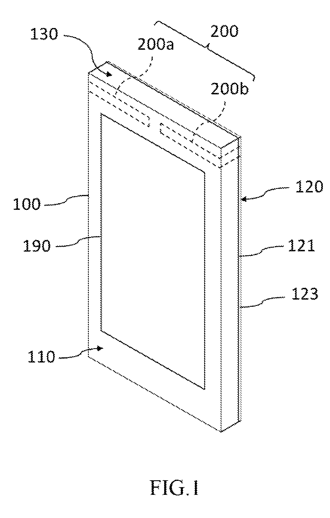
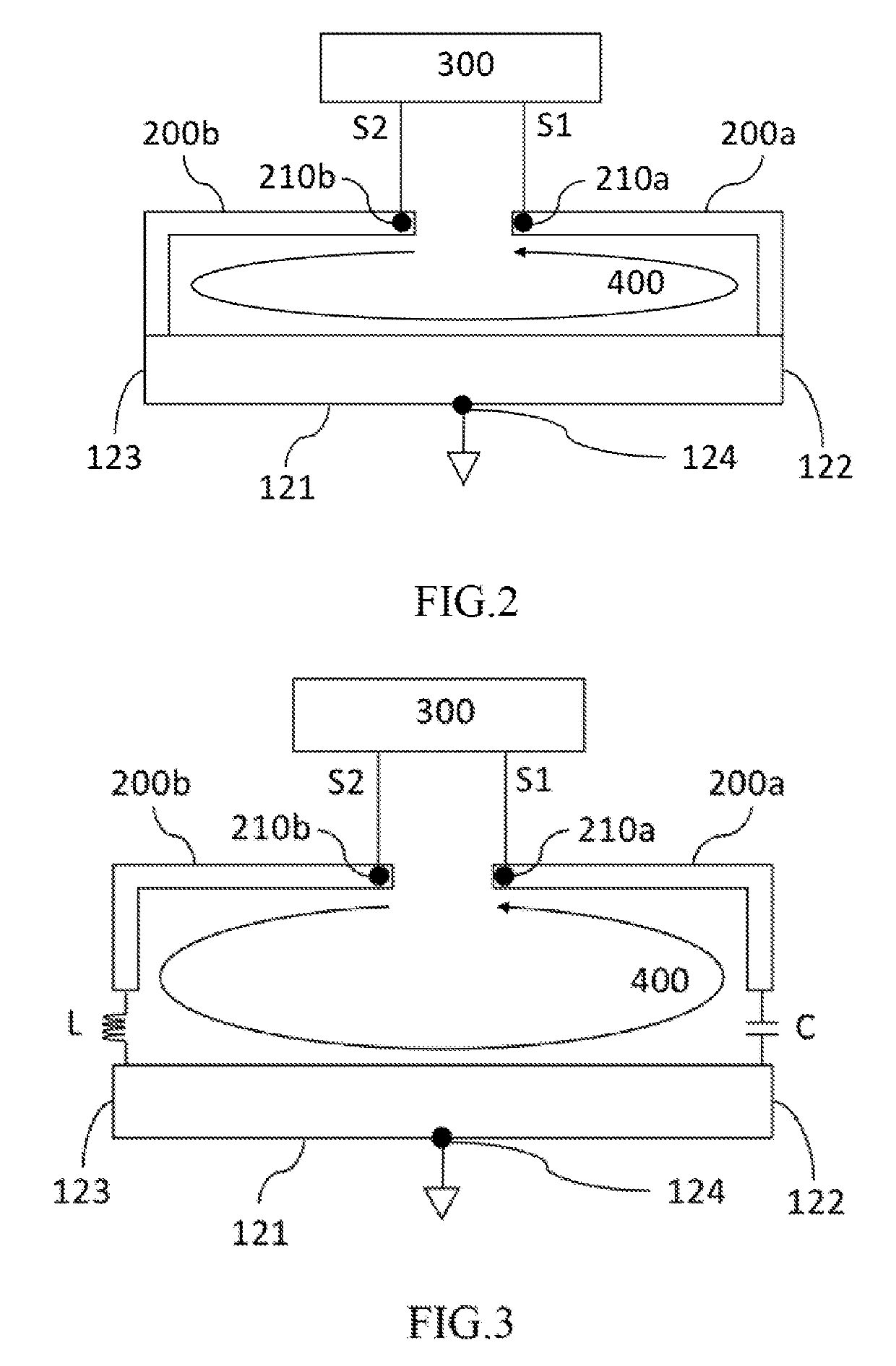
[0017]FIG. 1 is a perspective view of an electronic device in a In the embodiment, an electronic device includes a housing 100 and two conductive arms 200 (namely, a first conductive arm 200a and a second conductive arm 200b). The housing 100 includes a conducting portion 121. The conducting portion 121 is made of metal or other conductive materials. The first conductive arm 200a, the conducting portion 121 and the second conductive arm 200b are coupled in sequence to form a current loop 400 (as shown in FIG. 2). The housing 100 includes a front cover 110 and a back cover 120 that are opposite to each other. The back cover 120 includes the conducting portion 121. In an embodiment, considering the appearance of the housing, a great part or a main part of the two conductive arms 200 is disposed at the front cover 110. In an embodiment, the two conductive arms 200 is disposed at an outer / inner surface of the front cover 110, or embedded at the front cover 110, or disposed in the housi...

second embodiment

[0025]FIG. 3 is a top view of a current loop 400 of an electronic device in a In FIG. 3, in the embodiment, the first conductive arm 200a is coupled to the conducting portion 121 via the capacitor C, and the second conductive arm 200b is coupled to the conducting portion 121 via the inductor L. With the configuration of the capacitor C and the inductor L, an impedance matching between the current loop 400 and the near field communication circuit 300 is adjusted. In an embodiment, the first conductive arm 200a is coupled to the conducting portion 121 via the inductor L, and the second conductive arm 200b is coupled to the conducting portion 121 via the capacitor C. In other words, the first conductive arm 200a and the second conductive arm 200b are coupled to the conducting portion 121 via the capacitor C or the inductor L, respectively.

third embodiment

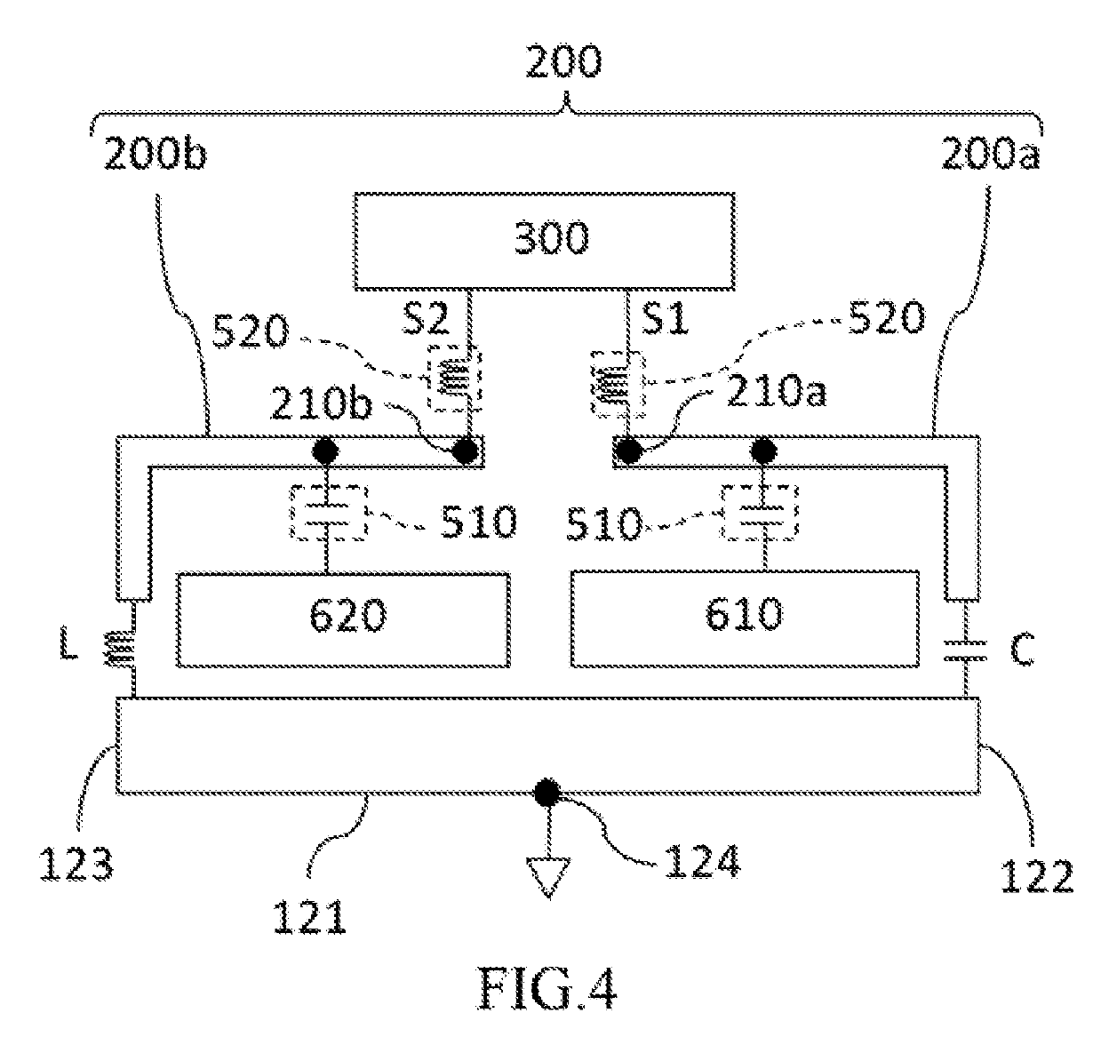
[0026]FIG. 4 is a top view of a current loop 400 of an electronic device in a In FIG. 4, the electronic device further includes a plurality of non-NFC circuits. In the embodiment, the non-NFC circuits is a Wi-Fi circuit 610 and a mobile communication circuit 620. The Wi-Fi circuit 610 is coupled to one of the conductive arms 200 (that is, the first conductive arm 200a) via a first energy storage component 510. The mobile communication circuit 620 is coupled to another conductive arm 200 (that is, the second conductive arm 200b) via another first energy storage component 510. The near field communication circuit 300 is coupled to the first conductive arm 200a and the second conductive arm 200b via a second energy storage component 520, respectively. In the embodiment, the first energy storage component 510 is a capacitor, and the second energy storage component 520 is an inductor accordingly. Since the capacitor supports a high-frequency signal, the inductor supports a low-frequency...


PUM


Abstract

An electronic device is provided. The An electronic device comprises a near field communication (NFC) circuit for transmitting a set of near field communication differential signals including a first differential signal and a second differential signal; a housing including a conducting portion with a ground point, a first side and a second side opposite to the first side; and two conductive arms. A current loop is formed by the conductive arm and the conducting portion, and a potential of the ground point is equal to a median potential of the current loop.

Description

CROSS-REFERENCE TO RELATED APPLICATION[0001]This application claims the priority benefit of China application serial No. 201610329442.X, filed on May 18, 2016. The entirety of the above-mentioned patent application is hereby incorporated by references herein and made a part of specification.BACKGROUND OF THE INVENTIONField of the Invention[0002]The disclosure relates to an electronic device and, more specifically, to an electronic device with a near field communication circuit (NFC).Description of the Related Art[0003]Currently, housings of most electronic devices are made of metal. To avoid the shielding to the transmission of wireless communication signals from the metal materials, the hole(s) or aperture(s) is usually formed on a portion of the housing that corresponds to the antenna to allow the signals to go through. However, with the hole(s) or aperture(s), the aesthetic feeling of the appearance of the electronic device is affected.BRIEF SUMMARY OF THE INVENTION[0004]Accordin...

Claims


Application Information

Patent Timeline
Patent Type & Authority Patents(United States)
IPC IPC(8): H01Q7/00H01Q5/314H04B5/02H01Q1/24H01Q1/22
CPCH01Q7/00H01Q1/2291H04B5/02H01Q5/314H01Q1/243H01Q1/36H01Q1/44H01Q1/48H01Q1/50
Inventor TSAI, CHIEN-HUNGLIEN, TE-LILO, WEI-CHENGLIAO, KUO-CHU
Owner ASUSTEK COMPUTER INC
Features
  • R&D
  • Intellectual Property
  • Life Sciences
  • Materials
  • Tech Scout
  • Unparalleled Data Quality
  • Higher Quality Content
  • 60% Fewer Hallucinations
Learn More