Method to make a photoconductor drum having an overcoat using a dual curing process

a photoconductor and overcoat technology, applied in the field of electrotrophotographic image forming devices, can solve the problems of mechanical abrasion of the surface layer of the photoconductor drum, scratches and abrasions of the organic photoconductor drum, and the use of organic photoconductor drums

Active Publication Date: 2019-05-14
CHARLES STARK DRAPER LABORATORY +1
View PDF6 Cites 4 Cited by
  • Summary
  • Abstract
  • Description
  • Claims
  • Application Information

AI Technical Summary

Problems solved by technology

Conversely, the surface of an organic photoconductor drums is typically comprised of a low molecular weight charge transport material, and an inert polymeric binder and are susceptible to scratches and abrasions.
Therefore, the drawback of using organic photoconductor drums typically arises from mechanical abrasion of the surface layer of the photoconductor drum due to repeated use.
Abrasion of photoconductor drum surface may arise from its interaction with print media (e.g. paper), paper dust, or other components of the electrophotographic image forming device such as the cleaner blade or charge roll.
The abrasion of photoconductor drum surface degrades its electrical properties, such as sensitivity and charging properties.
Electrical degradation results in poor image quality, such as lower optical density, and backgroun...

Method used


Image

  • Method to make a photoconductor drum having an overcoat using a dual curing process
  • Method to make a photoconductor drum having an overcoat using a dual curing process
  • Method to make a photoconductor drum having an overcoat using a dual curing process

Examples


Embodiment Construction

[0012]It is to be understood that the disclosure is not limited in its application to the details of construction and the arrangement of components set forth in the following description or illustrated in the drawings. The disclosure is capable of other embodiments and of being practiced or of being carried out in various ways. Also, it is to be understood that the phraseology and terminology used herein is for the purpose of description and should not be regarded as limiting. The use of “including,”“comprising,” or “having” and variations thereof herein is meant to encompass the items listed thereafter and equivalents thereof as well as additional items. Further, the terms “a” and “an” herein do not denote a limitation of quantity, but rather denote the presence of at least one of the referenced item.

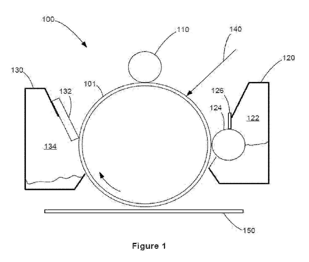
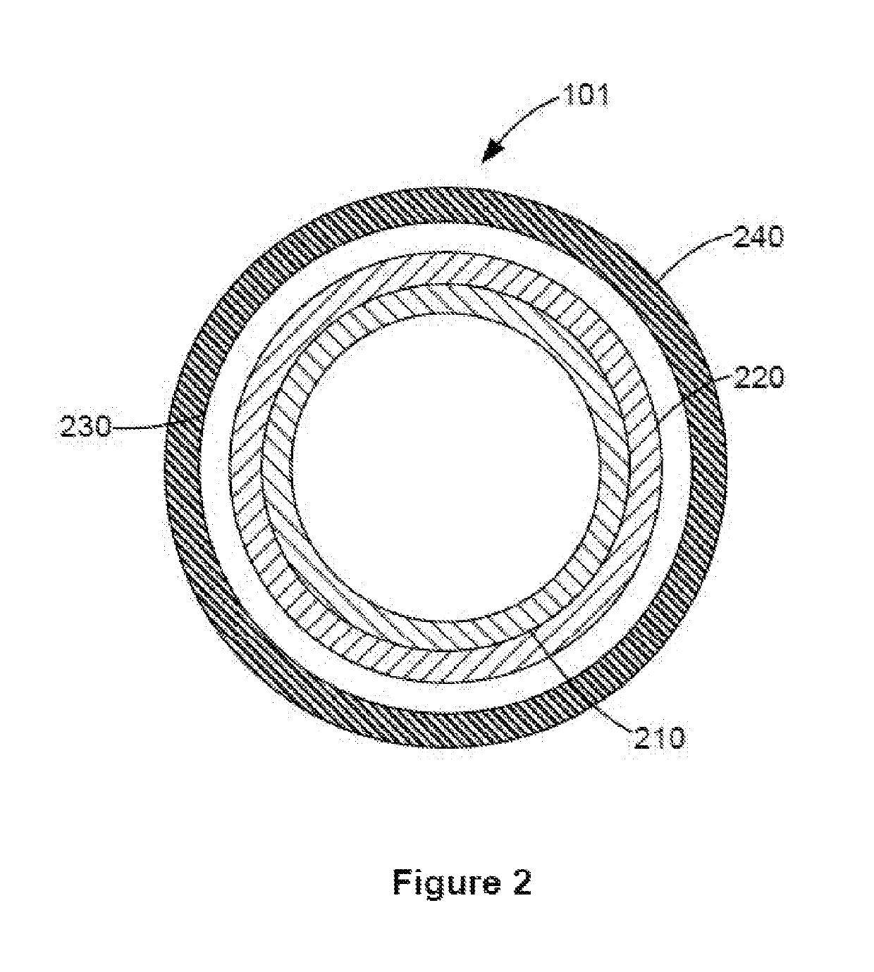
[0013]FIG. 1 illustrates a schematic representation of an example electrophotographic image forming device 100. Image forming device 100 includes a photoconductor drum 101, a charge ro...


PUM

PropertyMeasurementUnit
Temperatureaaaaaaaaaa
Irradiation doseaaaaaaaaaa

Abstract

A method of preparing an organic photoconductor drum having a protective overcoat on its outermost surface is provided. In an example embodiment, a photoconductor drum having an electrically conductive substrate, a charge generation layer, a charge transport layer and an outermost protective overcoat layer is provided. The photoconductor drum is cured using a two-step process. The first curing step applies either ionizing irradiation, such as with an electron beam or by gamma rays or applies non-ionizing irradiation such as ultraviolet light to the photoconductor drum. A mask is sized and placed over the print area of the initially cured photoconductor drum, thereby exposing the outermost edges of the photoconductor drum. The outer edges of the masked photoconductor drum is then exposed to a second curing step using ultraviolet light irradiation.

Description

CROSS REFERENCES TO RELATED APPLICATIONS[0001]NoneBACKGROUND1. Field of the Disclosure[0002]The present disclosure relates generally to electrophotographic image forming devices, and more particularly to a method to make an organic photoconductor drum having a protective overcoat layer placed its outermost surface. A photoconductor drum having an electrically conductive substrate, a charge generation layer, a charge transport layer and a protective overcoat layer is provided. The protective overcoat is cured using a two-step process. The first curing step applies either ionizing irradiation, such as with an electron beam (‘EB’) or by gamma rays or applies non-ionizing irradiation such as ultraviolet (‘UV’) light to the overcoated photoconductor drum. A mask or shield is sized to be placed over the print area of the initially cured photoconductor drum, thereby exposing the outermost edges of the photoconductor drum. The masked photoconductor drum is then exposed to a second curing st...

Claims


Application Information

Patent Timeline
IPC IPC(8): G03G7/00B05D1/18B05D3/06B05D1/02G03G5/05G03G5/147
CPCG03G7/0006G03G5/147G03G5/0525B05D3/067B05D3/068B05D1/02B05D1/18G03G5/14791
Inventor LUO, WEIMEIBELLINO, MARK THOMASHROBSKY, RUDOLPH WAYNE
Owner CHARLES STARK DRAPER LABORATORY
Why Eureka
Try Eureka