Liquid crystal display device

a liquid crystal display and display panel technology, applied in non-linear optics, instruments, optics, etc., can solve the problems of black stain, affecting the display area, and lowering the display image quality, so as to maximize the display area of the liquid crystal display panel and minimize the external form of the panel

Active Publication Date: 2019-06-11
JAPAN DISPLAY INC
View PDF16 Cites 0 Cited by
  • Summary
  • Abstract
  • Description
  • Claims
  • Application Information

AI Technical Summary

Benefits of technology

[0008]There is a growing need to maximize the display area of the liquid crystal display panel while minimizing the external form of the panel. To do so involves minimizing the width between the edge of the display area and that of the liquid crystal display panel, i.e., the width of the frame. As a result, the ions supposed to be collected outside the display area tend to move back to the periphery of the display area and are likely to trigger a black stain there.
[0010]The present disclosure has been made in view of the above circumstances and provides arrangements for preventing the ions trapped outside the display area from moving back to the display area while protecting the display area from being affected by the voltage impressed to the ion trap electrodes formed outside the display area.

Problems solved by technology

As a result, the ions supposed to be collected outside the display area tend to move back to the periphery of the display area and are likely to trigger a black stain there.
Also, when the width of the frame is reduced, the voltage impressed to ion trap electrodes formed in the frame area can affect the display area and lower display image quality.

Method used


Image

  • Liquid crystal display device
  • Liquid crystal display device
  • Liquid crystal display device

Examples


first embodiment

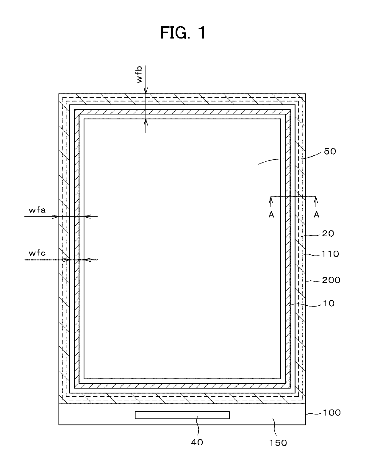
[0039]FIG. 1 is a plan view showing a liquid crystal display panel embodying the present disclosure and used on a mobile phone for example. In FIG. 1, a TFT substrate 100 and a counter substrate 200 are bonded together in the periphery thereof by the seal material 110, the two substrates having liquid crystal sandwiched therebetween. The TFT substrate 100 is formed to be larger than the counter substrate 200. That portion of the TFT substrate 100 which is not covered by the counter substrate 200 constitutes a terminal area 150. A driver integrated circuit (IC) 40 is disposed in the terminal area 150. A flexible wiring substrate for externally feeding power and signals to the liquid crystal display panel is connected to the terminal area 150.

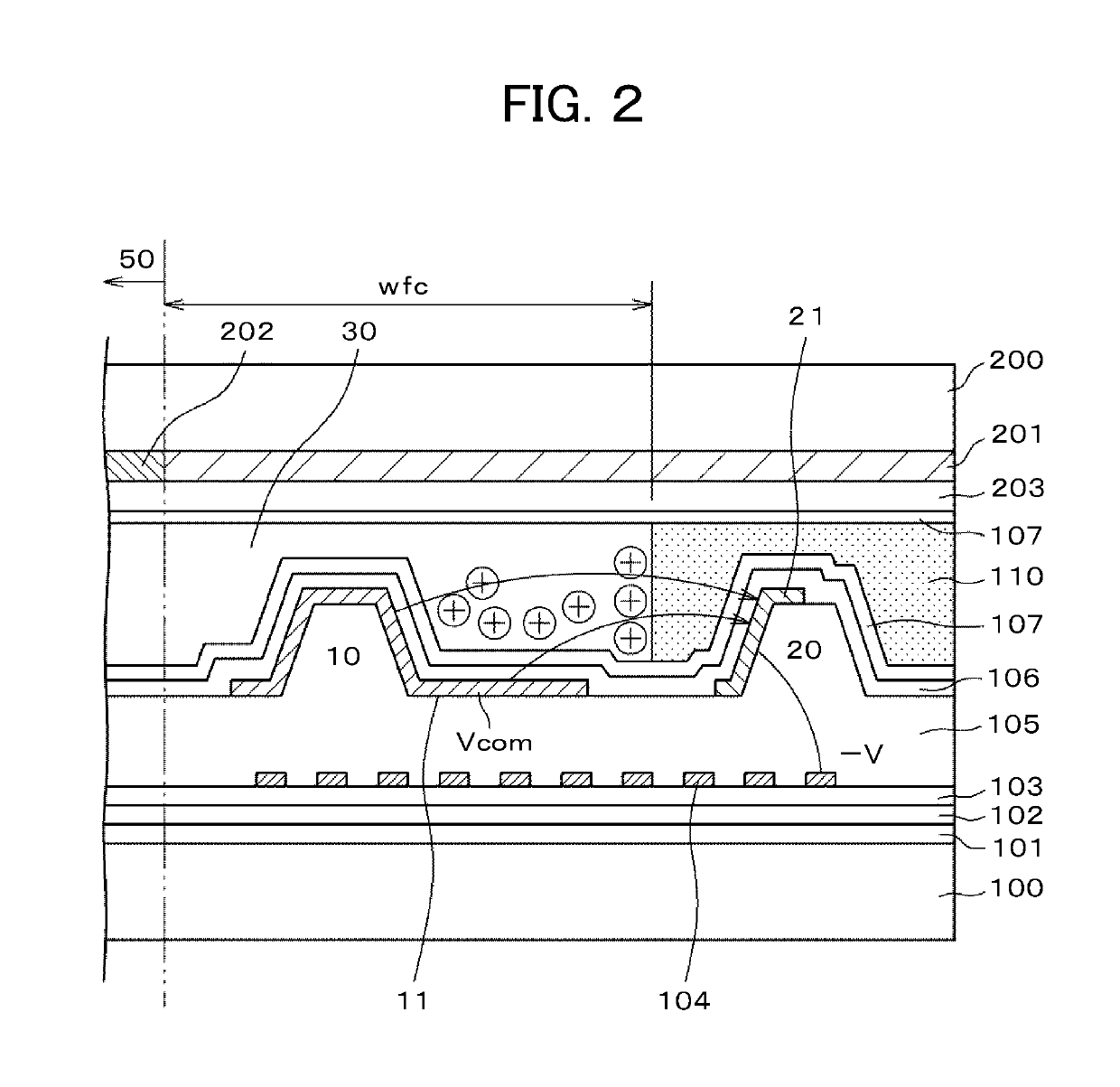
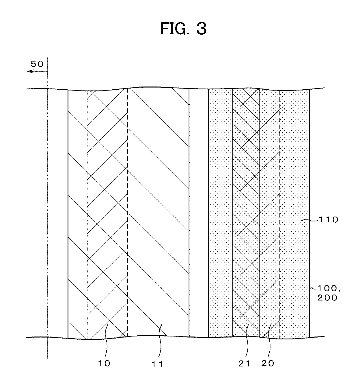
[0040]In FIG. 1, a second wall 20 topped by a second electrode is formed under the seal material 110 to trap ions. Also in FIG. 1, a first wall 10 topped by a first electrode is formed between the display area 50 and the seal material 110. This e...

second embodiment

[0071]A second embodiment defines where the first wall 10 is to be formed over a liquid crystal display panel as viewed in a plan view. In the structure of the first embodiment in FIG. 1, the first wall 10 is formed in a manner surrounding the entire display area 50. Meanwhile, the regions where ions aggregate are not necessarily along the entire periphery; the ions tend to aggregate in partial regions of the frame area. Where the first wall 10 is formed, it has a reduced distance to the counter substrate 200. That means it takes a longer time to fill the gap between the first wall 10 and the seal material 110 with liquid crystal. The second embodiment is intended to overcome this problem.

[0072]FIG. 9 shows an example in which the first wall 10 is formed with space in between. Whereas the first wall 10 in FIG. 9 is shown surrounding the display area 50, there are missing parts of the first wall 10 in FIG. 9. The liquid crystal may be injected through these missing parts to the side ...

third embodiment

[0076]The first embodiment and second embodiment above were described by assuming that the IPS liquid crystal display device is in use. However, the present disclosure is not limited to IPS devices but is also applicable to liquid crystal display devices operating on the twisted nematic (TN) method or the vertical alignment (VA) method, for example. A major difference between the IPS method and the TN or VA method (hereunder, simply called the VA method or the like) is that with the VA method or the like, the common electrode is formed over the counter substrate. That means only the pixel electrodes are formed on the side of the TFT substrate.

[0077]The pixel electrodes are formed over an insulating film and under an alignment film in contact with the latter. In devices using the VA method or the like, the only transparent electrodes on the side of the TFT substrate are the pixel electrodes. It follows that the second electrode disposed over the second wall and the first electrode di...


PUM

PropertyMeasurementUnit
width wfaaaaaaaaaaa
distance wfcaaaaaaaaaa
width wfbaaaaaaaaaa

Abstract

A liquid crystal display device is configured to prevent the appearance on its display of a black stain stemming from a drop in volume resistivity of liquid crystal caused by ions therein. The device includes a thin-film transistor (TFT) substrate and a counter substrate bonded together along the periphery thereof by a seal material. The TFT substrate and the counter substrate have liquid crystal sandwiched therebetween and include a display area. A second wall is formed outside the display area over the TFT substrate. A second electrode is formed over the second wall. A first wall is formed between the second wall and the display area. A first electrode is formed over the first wall. The first wall has a gap against the counter substrate.

Description

CLAIM OF PRIORITY[0001]The present application claims priority from Japanese Patent Application JP 2015-223742 filed on Nov. 16, 2015, the content of which is hereby incorporated by reference into this application.BACKGROUND OF THE INVENTION[0002]1. Field of the Invention[0003]The present disclosure relates to a display device. More particularly, the disclosure relates to a liquid crystal display device that provides against display unevenness attributable to ion aggregates.[0004]2. Description of the Related Art[0005]Liquid crystal display devices are generally configured to have a thin-film transistor (TFT) substrate disposed opposite to a counter substrate with liquid crystal sandwiched therebetween, the TFT substrate typically having pixel electrodes and TFTs formed thereon in a matrix pattern. The display device forms an image by suitably controlling the light transmittance of liquid crystal molecules per pixel.[0006]Liquid crystal includes impurities that tend to be ionized. I...

Claims


Application Information

Patent Timeline
Patent Type & Authority Patents(United States)
IPC IPC(8): G02F1/1343G02F1/1333G02F1/1339G02F1/1335G02F1/1341G02F1/1337
CPCG02F1/134363G02F1/1339G02F1/13394G02F1/13439G02F1/133308G02F1/133345G02F2201/121G02F1/1337G02F2201/123G02F1/1341G02F1/133512G02F1/133514G02F2001/13415G02F2001/133337G02F1/133337G02F1/13415
Inventor ASOZU, GENKI
Owner JAPAN DISPLAY INC
Why Eureka
Try Eureka