Liquid crystal display device and mother substrate thereof

a technology mother substrate, which is applied in non-linear optics, instruments, optics, etc., can solve the problems of short-circuiting between terminals, bad connection of terminals of invaded liquid crystal display panel, etc., and achieve the effect of reducing the manufacturing cost of liquid crystal display panel

Active Publication Date: 2019-02-19
JAPAN DISPLAY INC
View PDF4 Cites 0 Cited by
  • Summary
  • Abstract
  • Description
  • Claims
  • Application Information

AI Technical Summary

Benefits of technology

[0006]Obtaining numerous liquid crystal display panels from a single mother substrate helps reduce the manufacturing cost of the liquid crystal display panels. In order to cleave as many liquid crystal display panels as possible from the mother substrate, it is ideal to eliminate any gap between the liquid crystal display panels on the mother substrate.
[0007]Meanwhile, there is a strong need to maximize the display area of the liquid crystal display device while keeping its external size to predetermined dimensions. To satisfy this need requires minimizing the frame width of the device as well as the planar dimension of its terminal area. In the terminal area, the terminals are formed to supply power and signals to the liquid crystal display panel. With the liquid crystal display panels still on the mother substrate, the seal material or alignment film of a liquid crystal display panel could overflow and invade the terminal area of an adjacent liquid crystal display panel. If that happens, the terminals of the invaded liquid crystal display panel are vulnerable to bad connection.

Problems solved by technology

If that happens, the terminals of the invaded liquid crystal display panel are vulnerable to bad connection.
If ITO residues result from the patterning, they can lead to short-circuiting between terminals.

Method used


Image

  • Liquid crystal display device and mother substrate thereof
  • Liquid crystal display device and mother substrate thereof
  • Liquid crystal display device and mother substrate thereof

Examples


embodiment 1

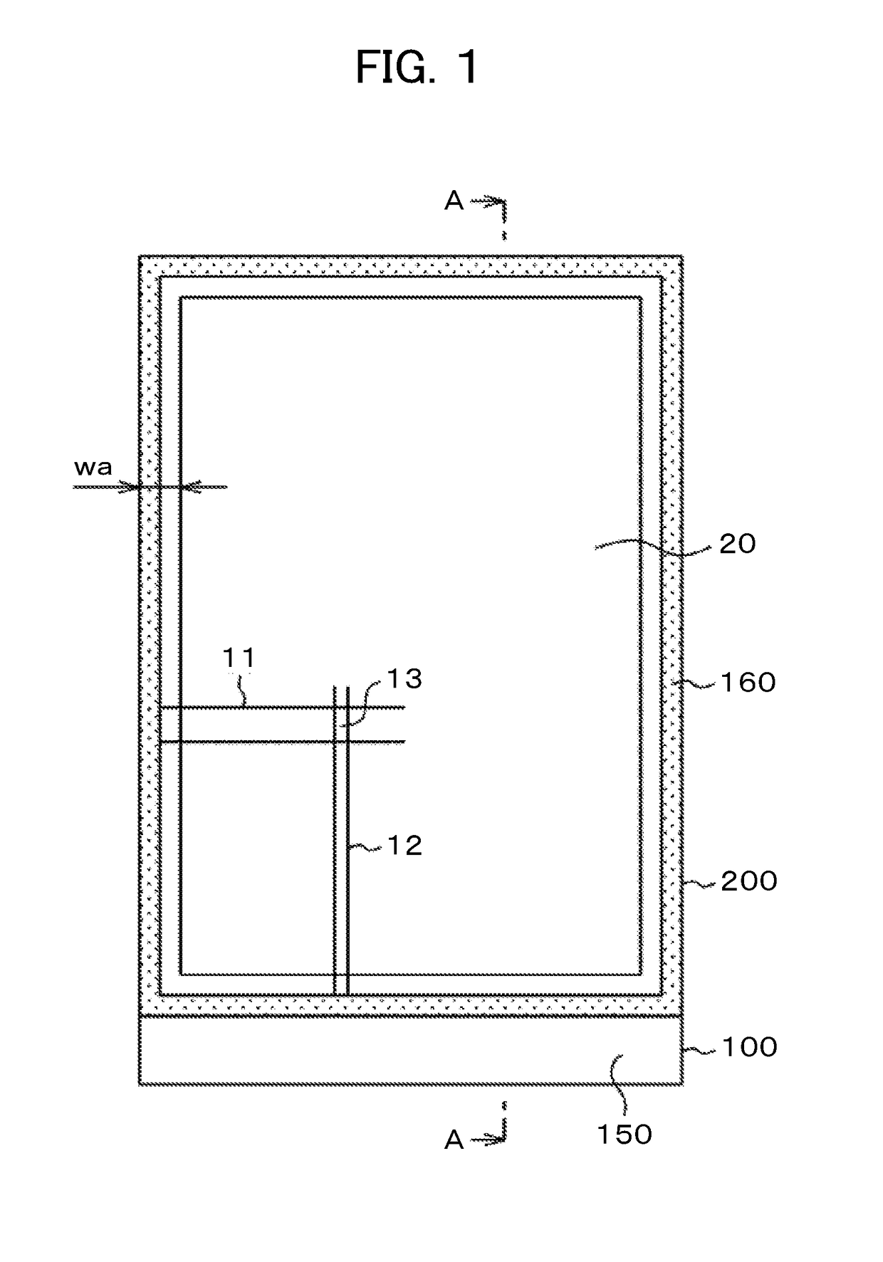
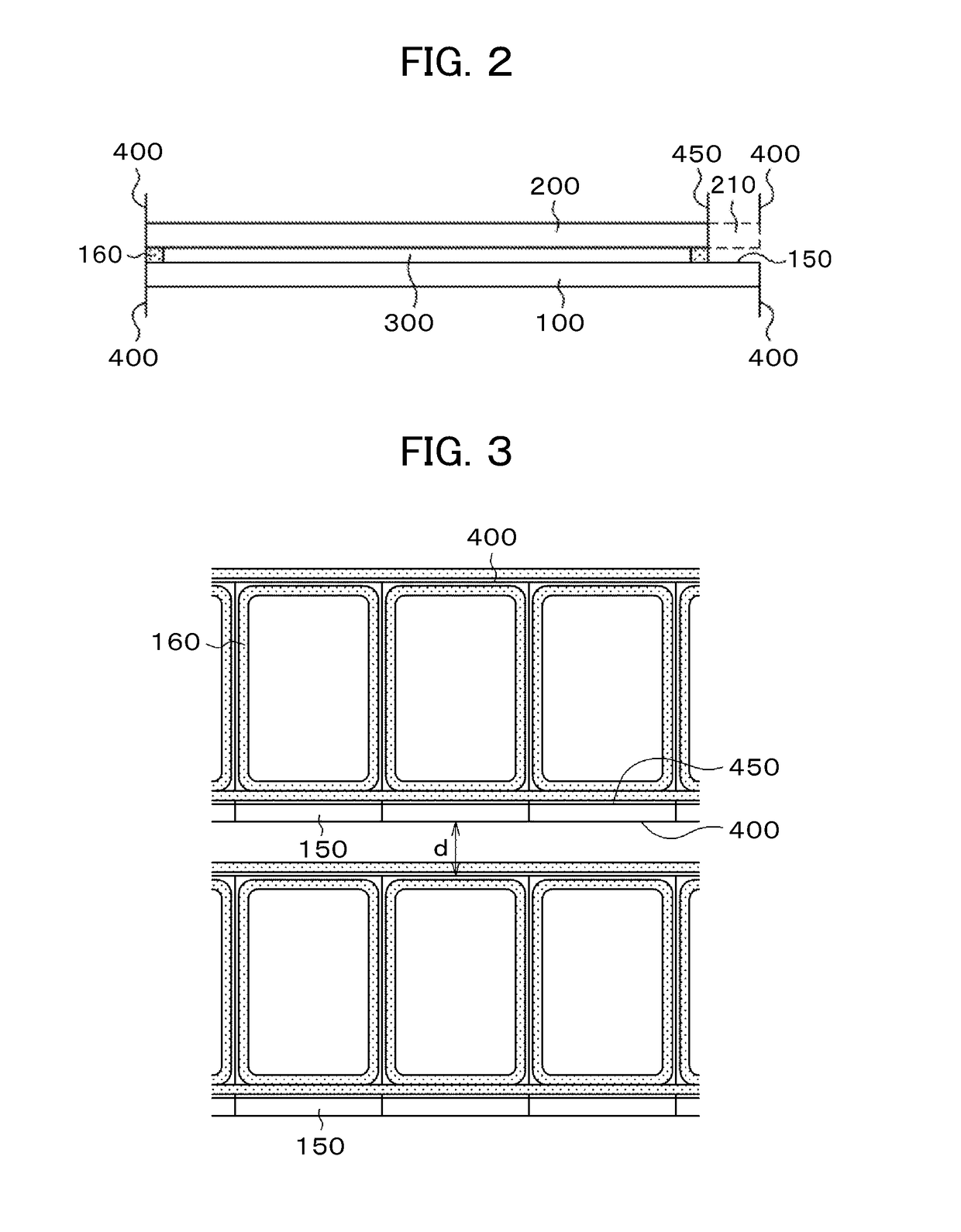
[0032]FIG. 1 is a plan view showing a typical liquid crystal display panel to which the present invention is applied, and FIG. 2 is a cross-sectional view taken on line A-A in FIG. 1. The liquid crystal display panel shown in FIG. 1 is used in a liquid crystal display device for use in a mobile phone, for example. In FIGS. 1 and 2, a TFT substrate 100 and a counter substrate 200 are bonded together by a seal material 160. The TFT substrate 100 and the counter substrate 200 have liquid crystal 300 sandwiched therebetween. The TFT substrate 100 is formed to be larger than the counter substrate 200. That portion of the TFT substrate 100 which is not overlaid with the counter substrate 200 constitutes a terminal area 150.

[0033]In FIG. 1, the periphery of a display area 20 constitutes a frame area. The seal material 160 is formed in the frame area. The liquid crystal display device such as one shown in FIG. 1 is required to have the largest possible display area 20. As a result, the widt...


PUM

PropertyMeasurementUnit
width waaaaaaaaaaa
width waaaaaaaaaaa
thickaaaaaaaaaa

Abstract

An object of this invention is to increase the number of liquid crystal display panels obtained from a mother substrate. There is provided a liquid crystal display device including a TFT substrate and a counter substrate bonded together by a seal portion formed along the periphery of the counter substrate, the TFT substrate having a terminal area formed in a portion thereof not opposed to the counter substrate. The TFT substrate has a bank-like organic passivation film formed along the edge of the terminal area. A stepped part is formed on the organic passivation film. The film thickness of the organic passivation film on the edge side of the stepped part is greater than the film thickness inside the stepped part.

Description

CLAIM OF PRIORITY[0001]The present application claims priority from Japanese Patent Application JP 2016-55280 filed on Mar. 18, 2016, the content of which is hereby incorporated by reference into this application.BACKGROUND OF THE INVENTION1. Field of the Invention[0002]The present invention relates to a display device. More particularly, the invention relates to techniques for obtaining as many liquid crystal display panels as possible from a mother substrate.2. Description of the Related Art[0003]Liquid crystal display devices are each constituted by a thin-film transistor (TFT) substrate and a counter substrate disposed opposite thereto. The TFT substrate has pixel electrodes and TFTs formed thereon in a matrix pattern. The TFT substrate and the counter substrate have liquid crystal sandwiched therebetween. The light transmittance of liquid crystal molecules is controlled per pixel in order to form images.[0004]It is not efficient to manufacture liquid crystal display panels one ...

Claims


Application Information

Patent Timeline
Patent Type & Authority Patents(United States)
IPC IPC(8): G02F1/1333G02F1/1335G02F1/1368G02F1/1345G02F1/1339
CPCG02F1/1339G02F1/1368G02F1/13394G02F1/133514G02F1/133345G02F1/133351G02F1/13458
Inventor ISHIKAWA, TOMOKAZUKURAMOTO, YUKIHASEGAWA, HITOMI
Owner JAPAN DISPLAY INC
Why Eureka
Try Eureka