Double-sided display and method of packaging the same

a display and double-sided technology, applied in the field of double-sided displays, can solve the problems of affecting the working life of the oled device, affecting the display life of the organic light emitting diode, and the long-term use of the display panel, so as to reduce the edge width of the double-sided display and prolong the display li

Active Publication Date: 2019-07-16
WUHAN CHINA STAR OPTOELECTRONICS TECH CO LTD
View PDF11 Cites 0 Cited by
  • Summary
  • Abstract
  • Description
  • Claims
  • Application Information

AI Technical Summary

Benefits of technology

[0051]Therefore, the double-sided OLED display of the present invention can protect the display from high-temperature damage and prolong the display life by disposing a glue on a side part of a packaging cover and thus away from a light-emitting surface. A thinning treatment is performed on the side part of the packaging cover and is beneficial to reduce an edge width of the double-sided display.

Problems solved by technology

However, these metals used for the cathode, such as aluminum, magnesium, calcium, etc., are generally more active and easy to react with water vapor infiltrated therein, thereby affecting a working life of the OLED devices.
The light emitting layer is damaged when a high temperature is used on the sealing portion, thereby affecting the displaying life of the organic light emitting diode.
Therefore, the conventional technology has the following technical problems that: the conventional double-sided OLED display devices are conventionally packaged, which is disadvantageous to a long-term use of the display panel and needs to be improved.

Method used


Image

  • Double-sided display and method of packaging the same
  • Double-sided display and method of packaging the same
  • Double-sided display and method of packaging the same

Examples


embodiment 1

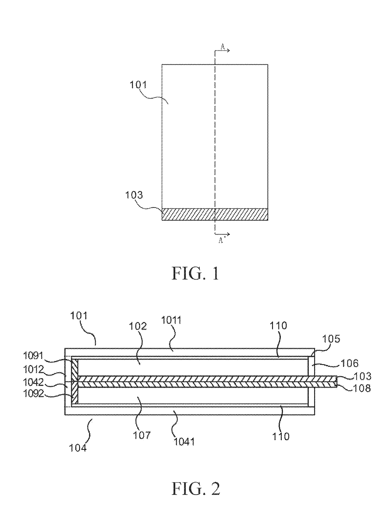
[0068]Refer to FIG. 1, which is a top view of a double-sided OLED display of the present invention.

[0069]As shown in FIG. 1, an upper packaging cover 101 is included. A first light emitting display portion is fixed in the upper packaging cover 101. The first light emitting display portion includes a first light emitting layer and a first substrate 103 located on a bottom part of the first light emitting layer. An end portion of the first substrate 103 is extended from an end of the upper packaging cover 101 to bind a display control device.

[0070]As shown in FIG. 2, which is a cross-sectional diagram along line A-A′ in FIG. 1, an upper packaging cover 101 and a lower packaging cover 104 are included. A lower surface of the upper packaging cover 101 is closely attached to an upper surface of the lower packaging cover 104. The upper packaging cover 101 is combined with the lower packaging cover to form a receiving chamber which is used to receive the first light emitting display portio...

embodiment 2

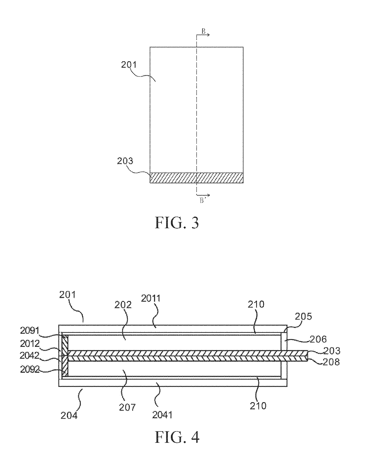
[0077]Refer to FIG. 3, which is a top view of a double-sided OLED display of the present invention.

[0078]As shown in FIG. 3, an upper packaging cover 201 is included. A first light emitting display portion is fixed in the upper packaging cover 201. The first light emitting display portion includes a first light emitting layer and a first substrate 203 located on a bottom part of the first light emitting layer. An end portion of the first substrate 203 is extended from an end of the upper packaging cover 201 to bind a display control device.

[0079]As shown in FIG. 4, which is a cross-sectional diagram along line B-B′ in FIG. 3. An upper packaging cover 201 and a lower packaging cover 204 are included. A lower surface of the upper packaging cover 201 is closely attached to an upper surface of the lower packaging cover 204. The upper packaging cover 201 is combined with the lower packaging cover 204 to form a receiving chamber which is used to receive the first light emitting display po...

embodiment 3

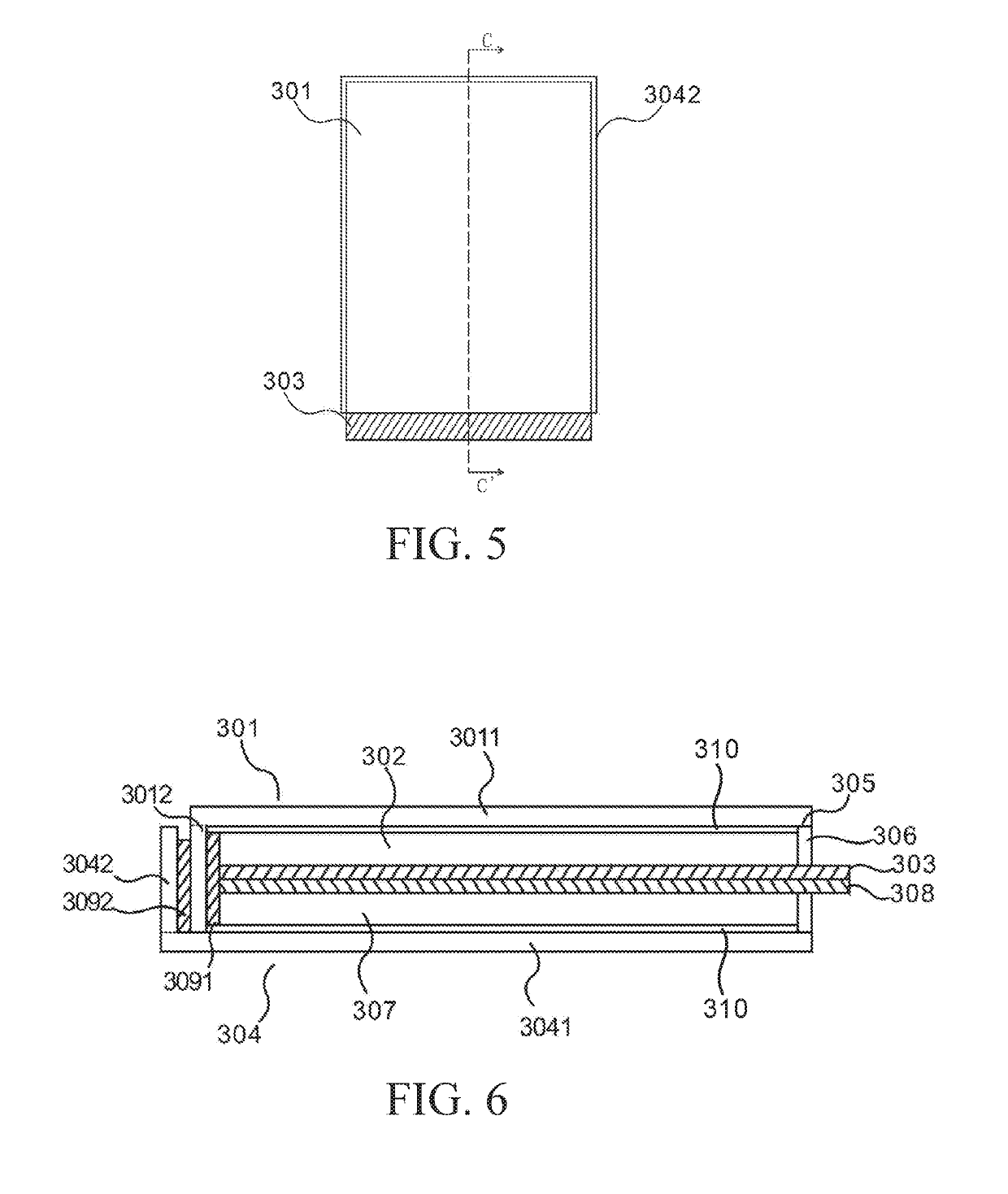
[0086]Refer to FIG. 5, which is a top view of a double-sided OLED display of the present invention.

[0087]As shown in FIG. 5, an upper packaging cover 301 is included. A first light emitting display portion is fixed in the upper packaging cover 301. The first light emitting display portion includes a first light emitting layer and a first substrate 303 located on a bottom part of the first light emitting layer. An end portion of the first substrate 303 is extended from an end of the upper packaging cover 301 to bind a display control device.

[0088]As shown in FIG. 6, which is a cross-sectional diagram along line C-C′ in FIG. 5, an upper packaging cover 301 and a lower packaging cover 304 are included. The upper packaging cover 301 and the lower packaging cover 304 are engaged with each other, i.e., the upper packaging cover 301 is partly or entirely located in an inner part of the lower packaging cover 304. The upper packaging cover 301 is combined with the lower packaging cover 304 t...


PUM


Abstract

A double-sided OLED packaging structure is provided and has an upper plate and a lower plate. Edges of each of the upper plate and the lower plate has a bending structure disposed thereon. A packaging glue is disposed on an inner side of the bending structure, such that two light emitting display portions are corresponding to and connected to each other by the packaging glues and the bending structures. Therefore, the double-sided OLED packaging structure can protect an organic light-emitting layer from high-temperature damage and prolong the display life by disposing the packaging glue on a side part of the packaging cover and thus away from a light-emitting surface.

Description

FIELD OF THE INVENTION[0001]The present invention relates to a technical field of displays, and more particularly to a double-sided display and a method of packaging the same.BACKGROUND OF THE INVENTION[0002]Organic light emitting diodes (OLED) are becoming more and more popular, and products such as mobile phones, media players, small entry-level televisions, and so on are the most significant. The OLED display is a self-luminous device with the advantages of bright colors, a high luminous efficiency, a light weight, a wide viewing angle, a fast response, a flexible preparation, etc. Simultaneously, electrons are injected into a cathode electrode when the OLED device works, which requires a work function of the cathode electrode to be as low as possible. However, these metals used for the cathode, such as aluminum, magnesium, calcium, etc., are generally more active and easy to react with water vapor infiltrated therein, thereby affecting a working life of the OLED devices. Therefo...

Claims


Application Information

Patent Timeline
Patent Type & Authority Patents(United States)
IPC IPC(8): H01L29/08H01L27/32H01L51/52H01L51/56
CPCH01L27/3267H01L51/5246H01L51/56H01L2251/5323H01L2227/323H10K59/128H10K50/8426H10K2102/3031H10K71/00H10K59/1201
Inventor TANG, YUEJUN
Owner WUHAN CHINA STAR OPTOELECTRONICS TECH CO LTD
Why Eureka
Try Eureka