Structure and method of forming transistor device having improved gate contact arrangement

a transistor and gate contact technology, applied in semiconductor devices, semiconductor/solid-state device details, electric discharge tubes, etc., can solve the problems of difficult overlay and contact issues, the inability to harness device improvements with decreased size, and the three-dimensional semiconductor transistors, transistors (finfets),

Active Publication Date: 2019-08-20
VARIAN SEMICON EQUIP ASSOC INC
View PDF10 Cites 3 Cited by
  • Summary
  • Abstract
  • Description
  • Claims
  • Application Information

AI Technical Summary

Benefits of technology

[0004]In various embodiments, device structures and method for forming improved gate contact arrangements are provided. is provided. A method may include providing a transistor structure on a substrate, where the transistor structure includes a semiconductor fin, a source / drain contact forming electrical contact with the semiconductor fin, and a gate conductor, disposed over the semiconductor fin, wherein the source drain contact and gate conductor are disposed in a trench. The method may further include directing angled ions to the trench, wherein the source / drain contact assumes a tapered shape.

Problems solved by technology

As semiconductor devices scale to smaller dimensions, the ability to harness device improvements with decreased size becomes more challenging.
The synthesis of three-dimensional semiconductor transistors, such as fin type field effect transistors (finFET), involves challenging overlay and contact issues.
For example, known FinFET based logic design rules do not allow placing gate contact over an active fin region, because an electrical short to source / drain (S / D) may arise.

Method used


Image

  • Structure and method of forming transistor device having improved gate contact arrangement
  • Structure and method of forming transistor device having improved gate contact arrangement
  • Structure and method of forming transistor device having improved gate contact arrangement

Examples


Embodiment Construction

[0015]The present embodiments will now be described more fully hereinafter with reference to the accompanying drawings, where some embodiments are shown. The subject matter of the present disclosure may be embodied in many different forms and are not to be construed as limited to the embodiments set forth herein. These embodiments are provided so this disclosure will be thorough and complete, and will fully convey the scope of the subject matter to those skilled in the art. In the drawings, like numbers refer to like elements throughout.

[0016]The present embodiments provide novel techniques and substrate structures to form devices, including three dimensional transistors, formed in a semiconductor substrate. As is known, three dimensional transistors, such as finFETs, may be arranged in circuitry to form various types of logic devices, as well as memory devices.

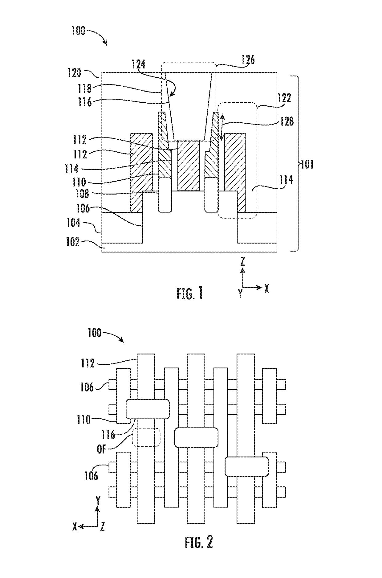
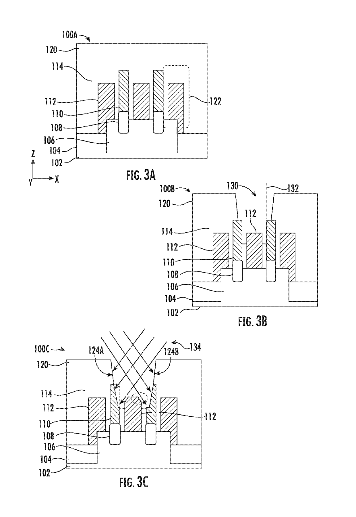
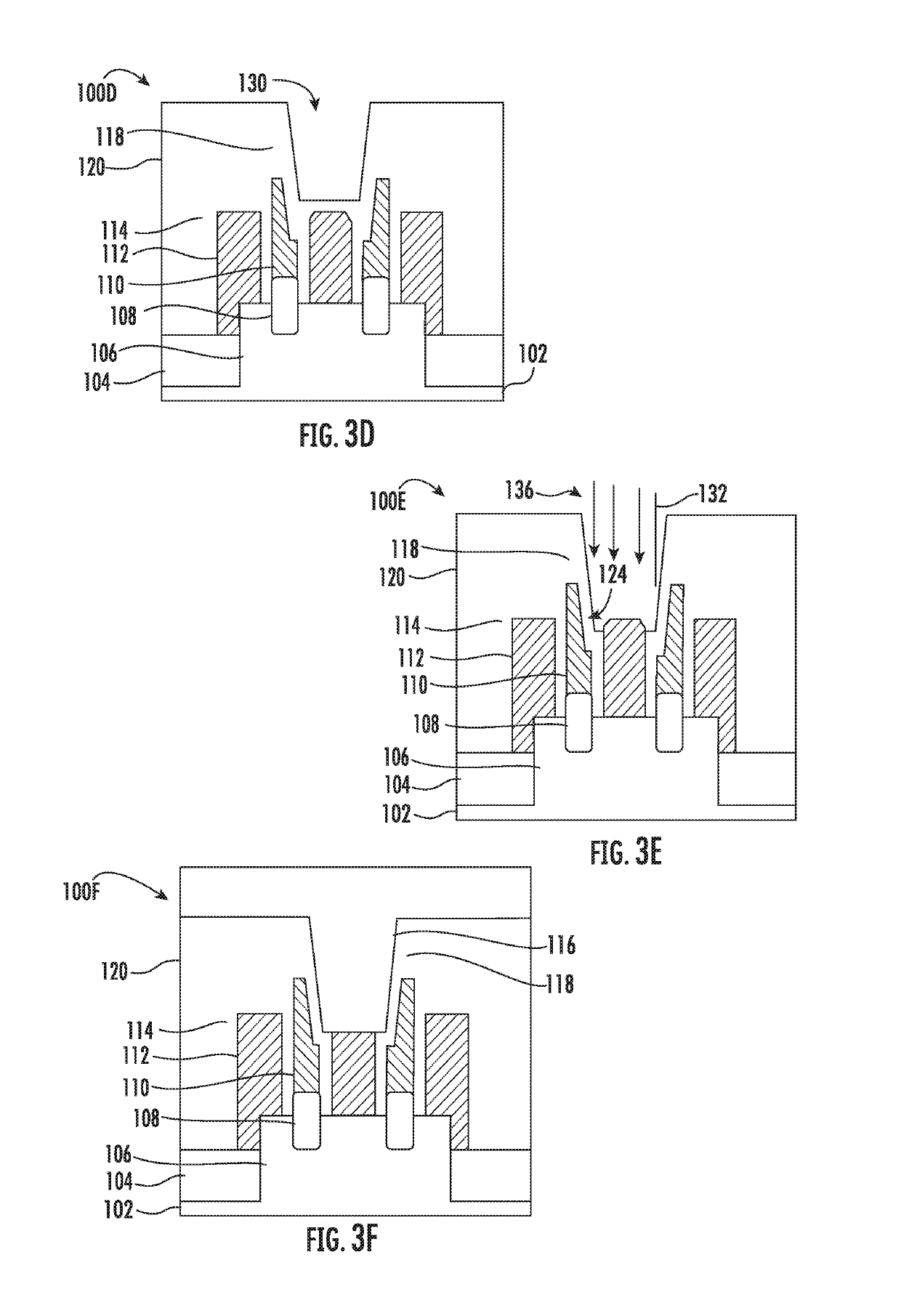
[0017]Turning now to FIG. 1 and FIG. 2 there is shown a device structure 100, according to embodiments of the disclosure. T...


PUM


Abstract

A method may include providing a transistor structure on a substrate, where the transistor structure includes a semiconductor fin, a source/drain contact forming electrical contact with the semiconductor fin, and a gate conductor, disposed over the semiconductor fin, wherein the source drain contact and gate conductor are disposed in a trench. The method may further include directing angled ions to the trench, wherein the source/drain contact assumes a tapered shape.

Description

FIELD[0001]The present embodiments relate to semiconductor device structures, and more particularly, to structures and processing for transistor devices.BACKGROUND[0002]As semiconductor devices scale to smaller dimensions, the ability to harness device improvements with decreased size becomes more challenging. The synthesis of three-dimensional semiconductor transistors, such as fin type field effect transistors (finFET), involves challenging overlay and contact issues. For example, known FinFET based logic design rules do not allow placing gate contact over an active fin region, because an electrical short to source / drain (S / D) may arise. This prohibition in gate contact arrangement incurs a scaling penalty of approximately 10% because of additional area entailed in gate contact placement to avoid the S / D region.[0003]With respect to these and other considerations, the present disclosure is provided.BRIEF SUMMARY[0004]In various embodiments, device structures and method for forming...

Claims


Application Information

Patent Timeline
Patent Type & Authority Patents(United States)
IPC IPC(8): H01L29/41H01L23/522H01L29/417H01L21/768H01L29/78H01L21/28H01L29/423H01L21/3213H01L21/67
CPCH01L29/41791H01L29/41775H01L21/76805H01L21/76804H01L29/785H01L21/28114H01L21/76814H01L21/67069H01L23/5226H01L29/42376H01L21/32136H01L29/66795H01L21/26586H01L21/76897H01L21/76883H01L21/76831H01J37/32357H01J37/32422
Inventor SUNG, MIN GYU
Owner VARIAN SEMICON EQUIP ASSOC INC
Why Eureka
Try Eureka