Input device and display device
a display device and input device technology, applied in the field of electrostatic capacitance type input devices, can solve the problems of reducing the detection sensitivity or an erroneous detection of the position, increasing the probability of failure of a part of the increased number of detection circuits, and reducing the visibility of the display image, so as to improve the reliability of the input device
- Summary
- Abstract
- Description
- Claims
- Application Information
AI Technical Summary
Benefits of technology
Problems solved by technology
Method used
Image

Examples
first embodiment
[0045]The technique described below is applicable to the input device provided to the on-cell type display device and the in-cell type display device. In this embodiment, to make operation of the input device easy to understand, there is described the example of the technique according to a part of the input device provided to the on-cell type display device. Among the electrostatic capacitance type input devices, an aspect applied to the input device of the mutual capacitance type is described in this embodiment while an aspect applied to the input device of the self-capacitance type is described as a modification.
[0046]
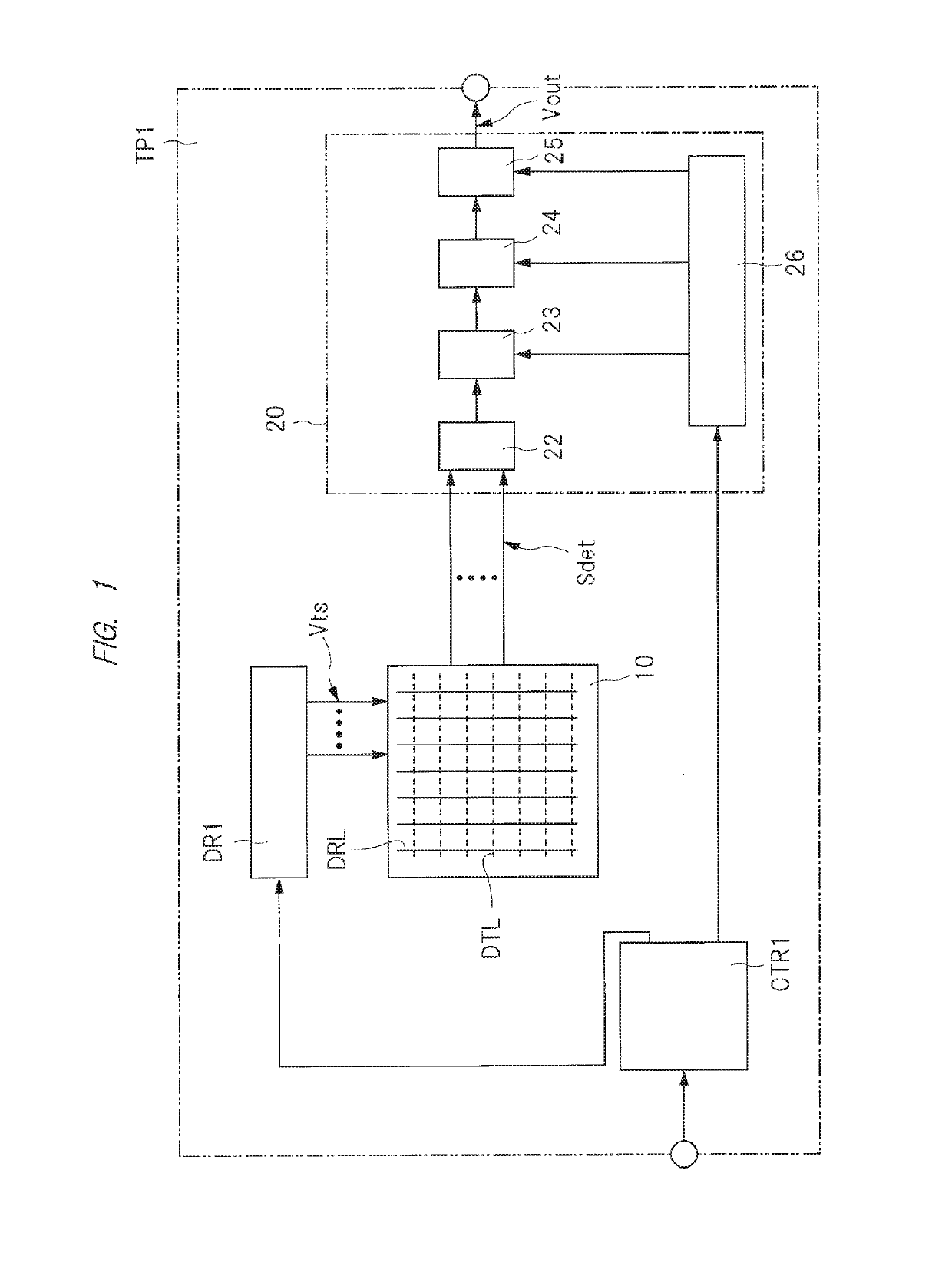
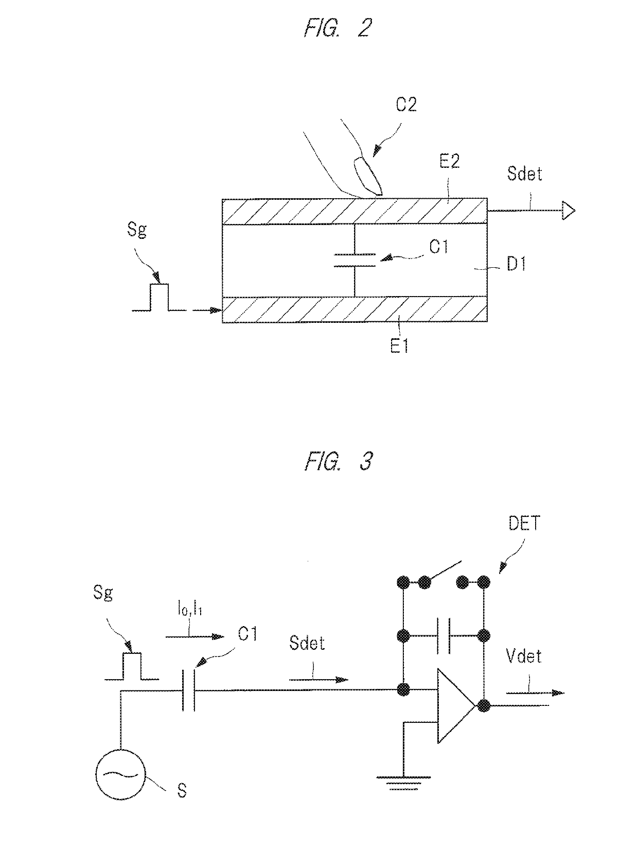
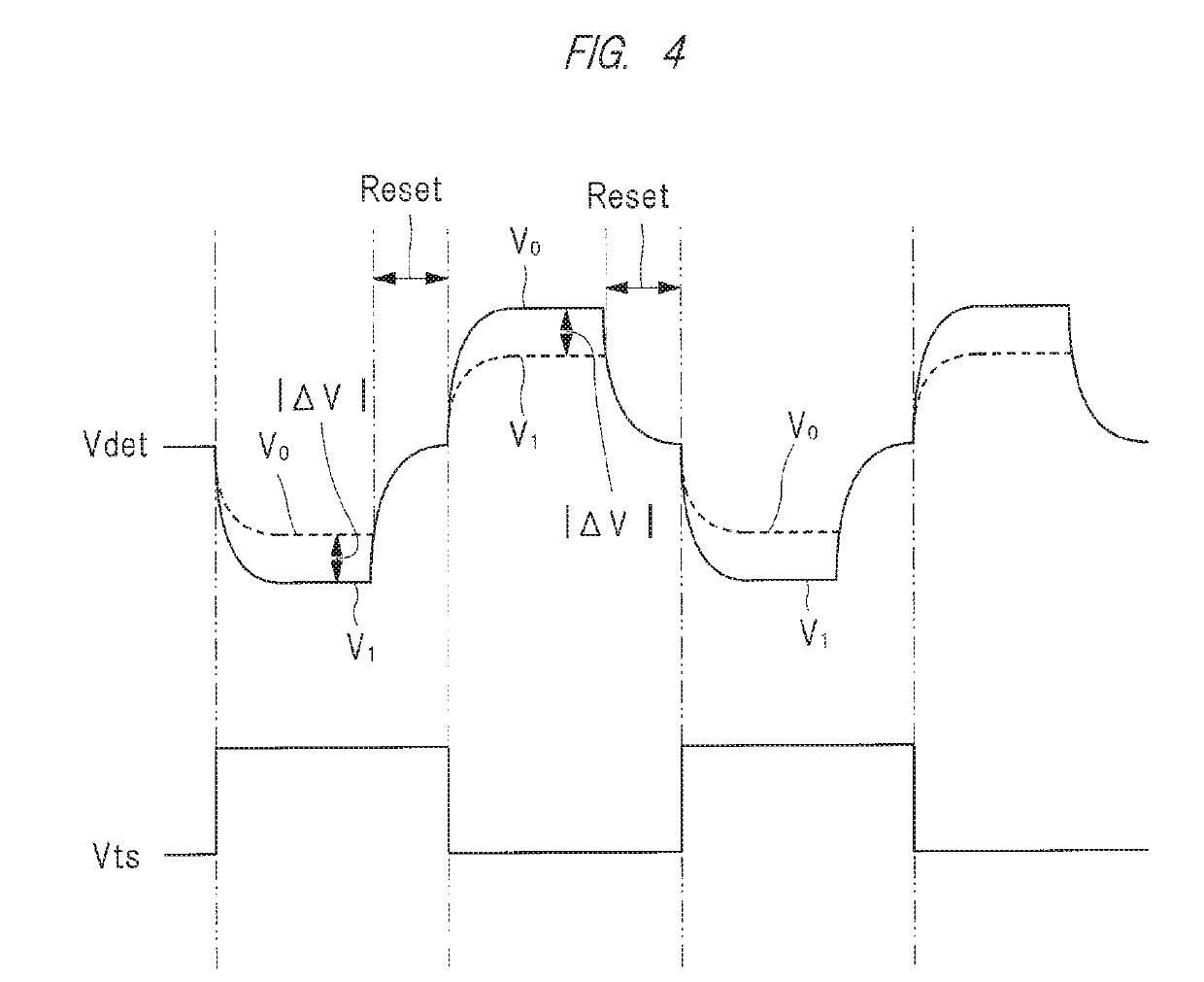
[0047]First, with reference to FIGS. 1 to 4, there is described a principle of input detection by an input device TP1 according to the first embodiment. FIG. 1 is a block diagram illustrating an exemplary configuration of the input device according to the first embodiment. FIG. 2 is an explanatory drawing illustrating a state in which a finger is in contact with or ...
second embodiment
[0120]In the second embodiment, there is described a method of suppressing an erroneous detection of an input position in an array direction of a plurality of driving electrodes DRL (Y axis direction in the example illustrated in FIGS. 5 and 7) by devising a method of selecting the plurality of driving electrodes DRL by the input detection driver DR1 illustrated in FIG. 1.
[0121]Note that, in the second embodiment, a method of driving the plurality of driving electrodes DRL is different from the aspect described in the first embodiment; however, a structure of the input device is the same as that of the aspect described in the above-described first embodiment. Thus, in the second embodiment, a difference from the first embodiment is mainly described, and any duplicated description is omitted in principle. In the second embodiment, the drawings described in the first embodiment are referred to as necessary.
[0122]In the above-described first embodiment, there is described the method of...
third embodiment
[0150]In the first embodiment and the second embodiment as well as the modifications of each of the embodiments, the aspect applied to the input device of the mutual capacitance type among the electrostatic capacitance type input devices has been described. In the third embodiment, an aspect applied to the input device of the self-capacitance type is described.
[0151]Note that the third embodiment is different from the aspect described in the first embodiment in that a signal is detected by the self-capacitance type; however, any other point except for the type, which is the electrostatic capacitance type, is the same as the aspect described in the first embodiment. Thus, in the third embodiment, a difference from the first embodiment is mainly described, and any duplicated description is omitted in principle. In the third embodiment, the drawings described in the first embodiment are referred to as necessary.
[0152]FIG. 19 is an explanatory drawing illustrating an electrical connecti...
PUM
 Abstract
Description
Claims
Application Information
 - R&D
- Intellectual Property
- Life Sciences
- Materials
- Tech Scout
- Unparalleled Data Quality
- Higher Quality Content
- 60% Fewer Hallucinations
Browse by: Latest US Patents, China's latest patents, Technical Efficacy Thesaurus, Application Domain, Technology Topic, Popular Technical Reports.
© 2025 PatSnap. All rights reserved.Legal|Privacy policy|Modern Slavery Act Transparency Statement|Sitemap|About US| Contact US: help@patsnap.com