Semiconductor memory device and method of programming multi bit data of the same

a memory device and semiconductor technology, applied in the field of semiconductor memory devices and a method of operating the same, can solve the problems of deteriorating loss of data stored therein in a non-powered condition, and non-volatile memory devices that perform at relatively slow read/write speed, etc., to achieve the effect of reducing the change of threshold voltage and improving the threshold voltage distribution of memory cells in semiconductor memory

Active Publication Date: 2019-12-31
SK HYNIX INC
View PDF28 Cites 0 Cited by
  • Summary
  • Abstract
  • Description
  • Claims
  • Application Information

AI Technical Summary

Benefits of technology

[0009]Exemplary embodiments of the present invention are directed to a semiconductor memory device that may improve threshold voltage distribution of memory cells and a method of operating the same.
[0010]A method of operating a semiconductor memory device in accordance with one embodiment of the present invention may include increasing threshold voltage of memory cells by performing an LSB program operation on the memory cells having first state, decreasing threshold voltage of memory cells to be programmed to second state of the memory cells to a level lower than a first level in unit of a memory cell for an MSB program operation, and increasing threshold voltage of memory cells to be programmed to third state of the memory cells to a level higher than a second level, which is higher than the first level, in unit of a memory cell for the MSB program operation.
[0013]In accordance with the embodiments of the present invention, threshold voltage distribution of memory cells in a semiconductor memory may be improved by reducing change of threshold voltage of the memory cells due to interferences between the memory cells.

Problems solved by technology

A volatile memory device may perform a read / write operation at a high speed, but may lose data stored therein in a non-powered condition.
Meanwhile, a non-volatile memory device performs at relatively slow speed in the read / write operation, but may maintain the stored data even when a power is blocked.
Therefore, threshold voltage distribution of the memory cells may be deteriorated due to interferences between the adjacent memory cells.

Method used


Image

  • Semiconductor memory device and method of programming multi bit data of the same
  • Semiconductor memory device and method of programming multi bit data of the same
  • Semiconductor memory device and method of programming multi bit data of the same

Examples


Embodiment Construction

[0028]Hereinafter, the preferred embodiments of the present invention will be explained in more detail with reference to the accompanying drawings. Although embodiments have been described with reference to a number of illustrative embodiments thereof, it should be understood that numerous other modifications and embodiments can be devised by those skilled in the art that will fall within the spirit and scope of the principles of this disclosure. Throughout the disclosure, reference numerals correspond directly to the like parts in the various figures and embodiments of the present invention. It is also noted that in this specification, “connected / coupled” refers to one component not only directly coupling another component but also indirectly coupling another component through an intermediate component. In addition, a singular form may include a plural form as long as it is not specifically mentioned in a sentence.

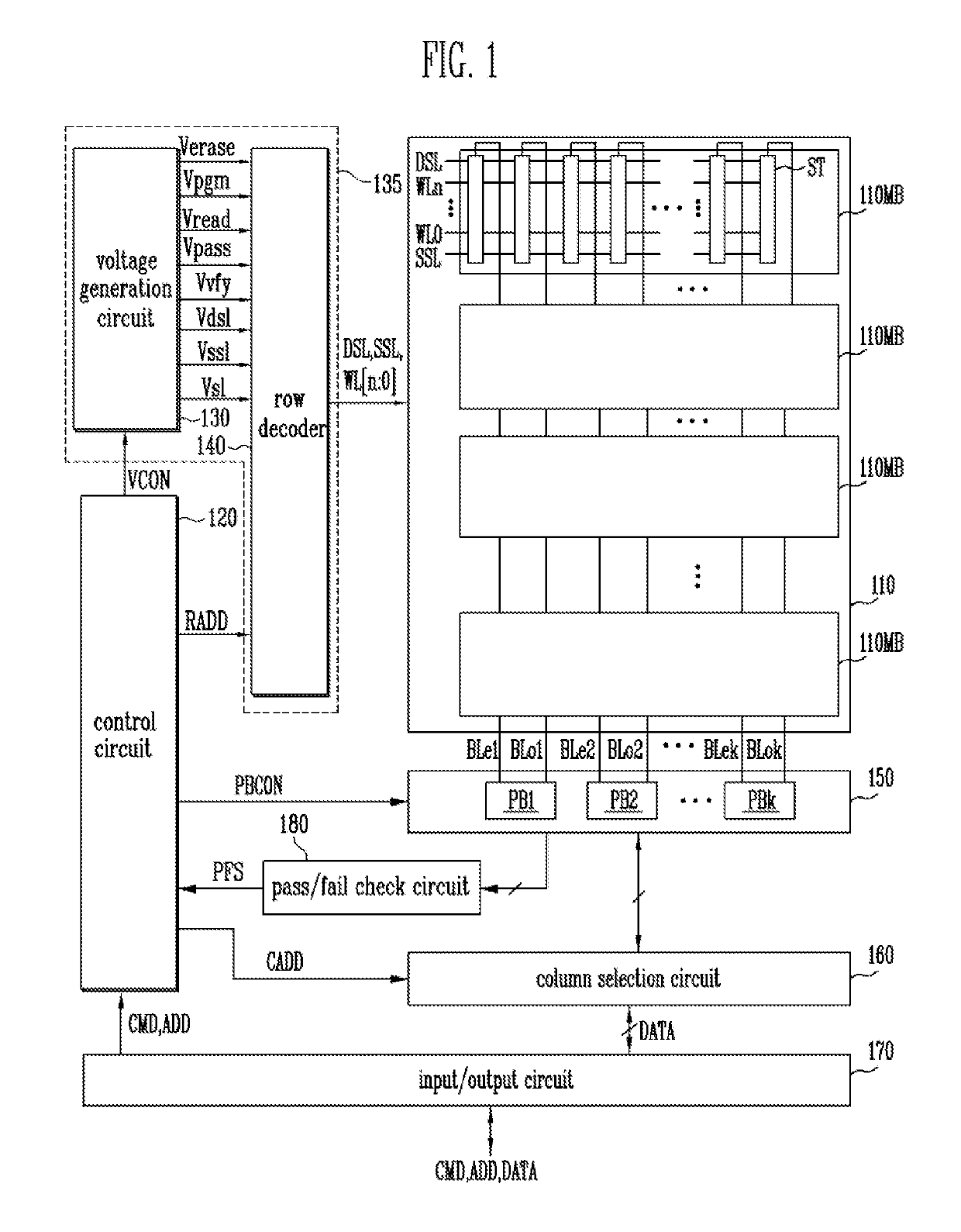
[0029]FIG. 1 is a block diagram illustrating a semiconductor memory ...


PUM


Abstract

A method of operating a semiconductor memory device may include increasing threshold voltage of memory cells by performing an LSB program operation on the memory cells having first state, decreasing threshold voltage of memory cells to be programmed to second state of the memory cells to a level lower than a first level in unit of a memory cell for an MSB program operation, and increasing threshold voltage of memory cells to be programmed to third state of the memory cells to a level higher than a second level, which is higher than the first level, in unit of a memory cell for an MSB program operation.

Description

CROSS-REFERENCE TO RELATED APPLICATION[0001]The present application claims priority to Korean Patent Application No. 10-2012-0124235, filed on Nov. 5, 2012, the disclosure of which is incorporated herein by reference in its entirety.BACKGROUND[0002]Field of Invention[0003]Exemplary embodiments of the present invention relate to semiconductor design technology, and more particularly, to a semiconductor memory device and a method of operating the same.[0004]Description of Related Art[0005]Semiconductor memory devices are classified into volatile memory devices and non-volatile memory devices.[0006]A volatile memory device may perform a read / write operation at a high speed, but may lose data stored therein in a non-powered condition. Meanwhile, a non-volatile memory device performs at relatively slow speed in the read / write operation, but may maintain the stored data even when a power is blocked. Accordingly, the non-volatile memory device is used for storing data, which is to be maint...

Claims


Application Information

Patent Timeline
Patent Type & Authority Patents(United States)
IPC IPC(8): G11C16/10G11C11/56G11C16/04
CPCG11C11/5642G11C11/5635G11C16/0483G11C2216/14G11C16/10G11C16/34
Inventor JEON, YOO NAM
Owner SK HYNIX INC
Why Eureka
Try Eureka