Non-volatile memory device, method of manufacturing the same and method of operating the same

a non-volatile memory and memory device technology, applied in the direction of semiconductor devices, electrical devices, transistors, etc., can solve the problems of affecting the operation of the device, and the poor properties of the unit cell, etc., to achieve the effect of reducing the disturbance of the implantation of hot electrons

Inactive Publication Date: 2010-04-13
SAMSUNG ELECTRONICS CO LTD
View PDF8 Cites 0 Cited by
  • Summary
  • Abstract
  • Description
  • Claims
  • Application Information

AI Technical Summary

Benefits of technology

[0011]Exemplary embodiments of the present invention provide a non-volatile memory device having good threshold voltage distribution and high durability.
[0012]Exemplary embodiments of the present invention provide a method of manufacturing a non-volatile memory device having good threshold voltage distribution and high durability.
[0013]Exemplary embodiments of the present invention provide a method of operating a non-volatile memory device having good threshold voltage distribution and high durability.
[0031]According to exemplary embodiments of the present invention, a depletion layer in an upper portion of a substrate, which is disposed under a sensing line, of the non-volatile memory device is always in an on-state when a gate voltage of more than about 0 V is applied to a memory transistor. Thus, even when electrons are trapped in the tunnel oxide layer, an on-current may not be decreased below a critical value. As a result, the durability of the non-volatile memory device may be enhanced.
[0033]Electron hole pair generation by a high electric field between an impurity region and a pocket well may be controlled by the depletion channel region. Thus, disturbance by the implantation of hot electrons may be reduced.

Problems solved by technology

The properties of the unit cells, however, may become poor as the sizes of the unit cells in the EEPROM device are reduced.
As a result, a voltage drop may occur during the programming or erasing of data.
When the memory transistor has the poorly distributed threshold voltage, a programming / erasing window margin may be decreased, so that accurately distinguishing data stored in a unit cell may be difficult.
Additionally, electrons may be trapped in the tunnel oxide layer of the memory transistor when data is repeatedly programmed or erased in the unit cell of the EEPROM device.
When the on-current is decreased, the decreased on-current may not be detected by a sense amplifier in a reading operation, so that the memory transistor may not accurately distinguish data.

Method used


Image

  • Non-volatile memory device, method of manufacturing the same and method of operating the same
  • Non-volatile memory device, method of manufacturing the same and method of operating the same
  • Non-volatile memory device, method of manufacturing the same and method of operating the same

Examples


Embodiment Construction

[0039]The present invention is described more fully hereinafter with reference to the accompanying drawings, in which exemplary embodiments of the present invention are shown. The present invention may, however, be embodied in many different forms and should not be construed as limited to the exemplary embodiments set forth herein. Rather, these exemplary embodiments are provided so that this disclosure will be thorough and complete, and will fully convey the scope of the present invention to those of ordinary skill in the art.

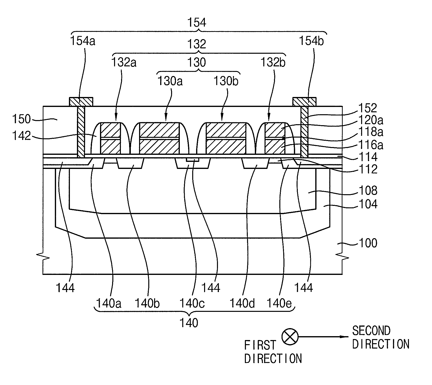
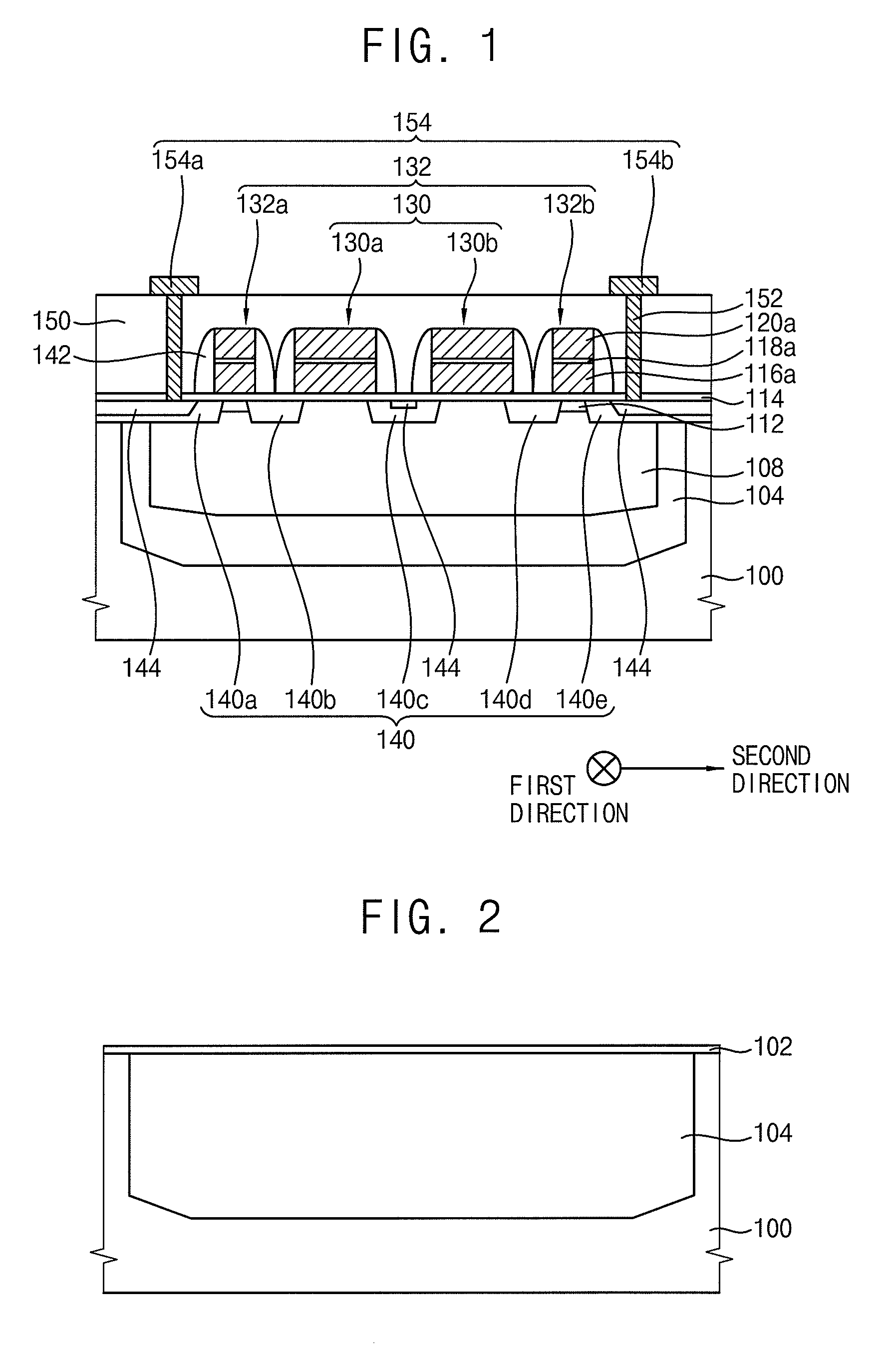
[0040]FIG. 1 is a cross-sectional view illustrating a non-volatile memory device in accordance with an exemplary embodiment of the present invention.

[0041]The non-volatile memory device may have a unit cell including a memory transistor and a select transistor. The memory transistor may store data and the select transistor may select a specific cell.

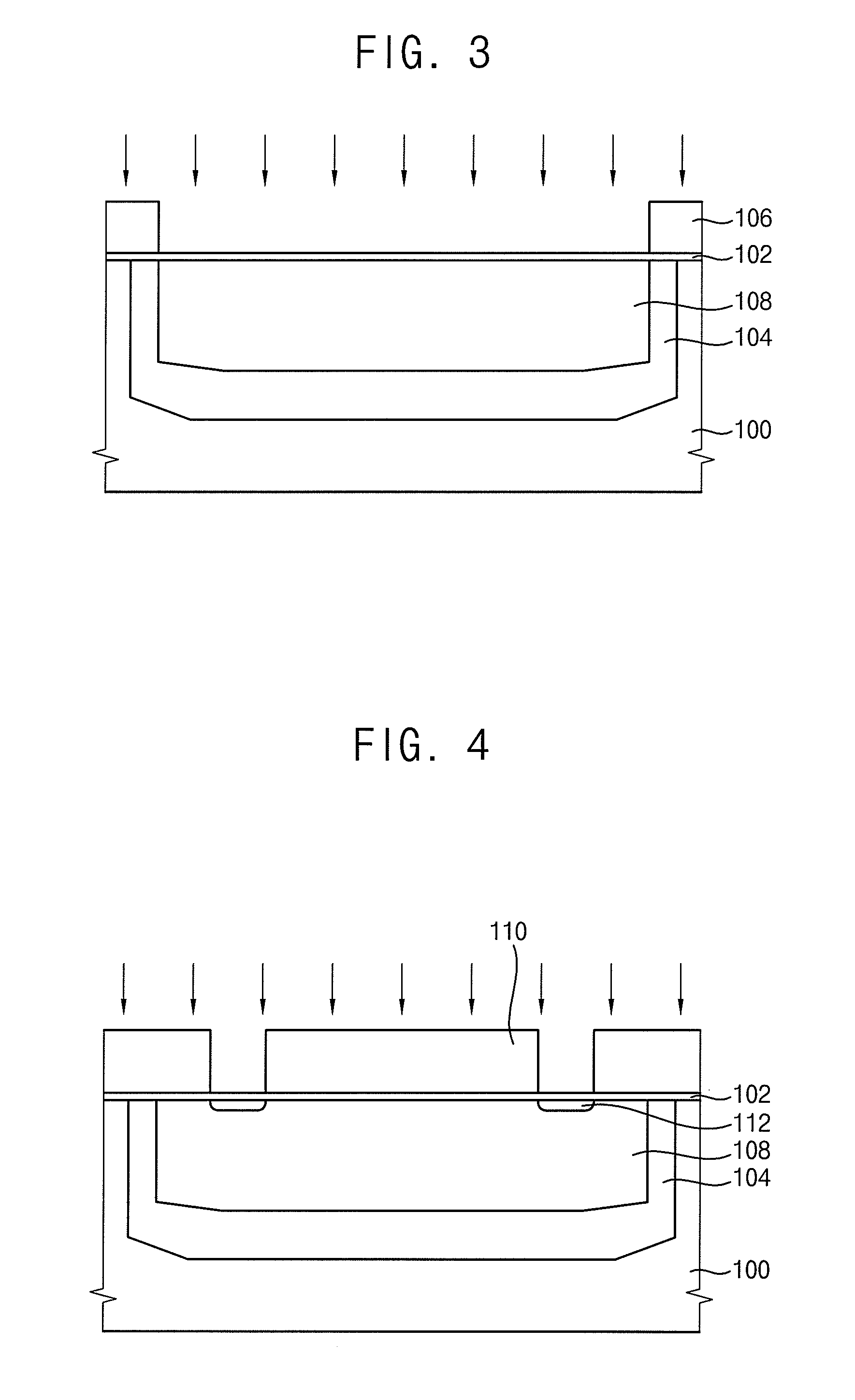
[0042]Referring to FIG. 1, a deep n-well 104 doped with n-type impurities is formed at a portion of a substrate ...


PUM


Abstract

A non-volatile memory device includes a first sensing line, a first word line, a depletion channel region, and impurity regions. The first sensing line and the first word line are formed adjacent to each other in parallel on a substrate. The first sensing line and the first word line have a tunnel oxide layer, a first conductive pattern, a dielectric layer pattern and a second conductive pattern sequentially stacked on the substrate. The depletion channel region is formed at an upper portion of the substrate under the first sensing line. The impurity regions are formed at upper portions of the substrate exposed by the first sensing line and the first word line.

Description

CROSS-REFERENCE TO RELATED APPLICATION[0001]This application claims priority under 35 U.S.C, §119 to Korean Patent Application No. 2006-99600, filed on Oct. 13, 2006 in the Korean Intellectual Property Office (KIPO), the contents of which are incorporated herein by reference in their entirety.BACKGROUND OF THE INVENTION[0002]1. Technical Field[0003]Exemplary embodiments of the present invention relate to a non-volatile memory device, a method of manufacturing the non-volatile memory device, and a method of operating the non-volatile memory device. More particularly, exemplary embodiments of the present invention relate to a non-volatile memory device including a memory transistor and a select transistor in a unit cell, a method of manufacturing the non-volatile memory device and a method of operating the non-volatile memory device.[0004]2. Discussion of Related Art[0005]Electrically erasable programmable read-only memory (EEPROM) devices, which are a type of non-volatile memory devi...

Claims


Application Information

Patent Timeline
Patent Type & Authority Patents(United States)
IPC IPC(8): H01L21/336
CPCH01L27/115H01L27/11524H01L27/11521H10B69/00H10B41/30H10B41/35H01L21/823493
Inventor YOO, HYUN-KHEHAN, JEONG-UKJEON, HEE-SEOGCHOI, SUNG-GONSEO, BO-YOUNGJEON, CHANG-MINRYU, JI-DO
Owner SAMSUNG ELECTRONICS CO LTD
Why Eureka
Try Eureka