Notch filter capable of partially suppressing/attenuating signal frequency components and associated filter circuit
a notch filter and signal frequency component technology, applied in the field of notch filtering, can solve the problems of narrow notch bandwidth of the conventional notch filter, and may not be suitable for signal processing circuits with specific requirements, and achieve the effect of adjusting the amount of attenuation appropriately and systematically
- Summary
- Abstract
- Description
- Claims
- Application Information
AI Technical Summary
Benefits of technology
Problems solved by technology
Method used
Image
Examples
first embodiment
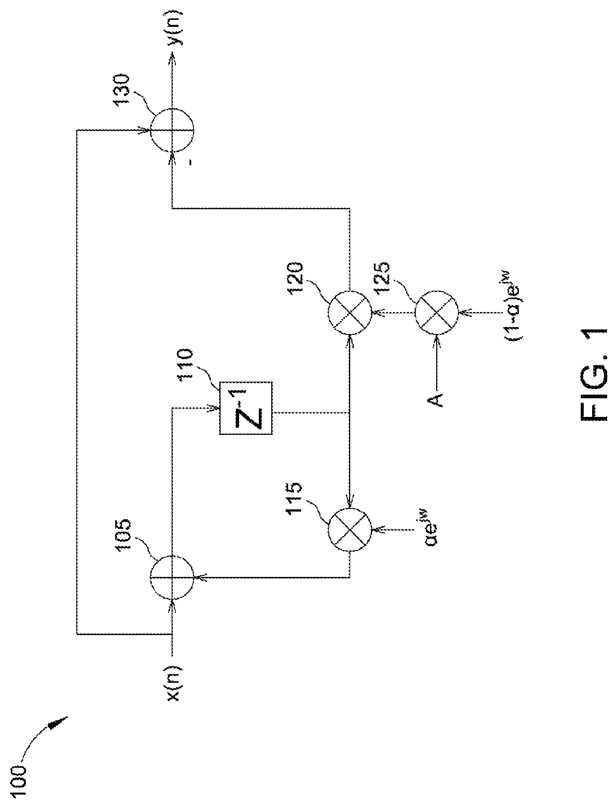
[0015]FIG. 1 shows a circuit diagram of a notch filter 100 according to the present invention. The notch filter 100 includes an adder 105, a delay circuit 110, multipliers 115, 120 and 125, and an adder 130. The adder 105 receives an input signal x(n) and an output signal of the multiplier 115. The delay circuit 110, coupled to the adder 105, serves as a buffer, and delays an output signal of the adder 105 by one unit time to generate a delayed signal. The multiplier 115, coupled to the delay circuit 110 and the adder 105, receives the delayed signal, and generates a product of a first parameter and the delayed signal as its output signal according to the first parameter. The first parameter is α×ejω, where α is a parameter for setting a notch band of the notch filter 100. In general, α is a value smaller than 1, and ω is a center frequency parameter of the notch bandwidth.
[0016]The multiplier 125 generates a product of an adjustable parameter A and a second parameter (1−α)×ejω as i...
second embodiment
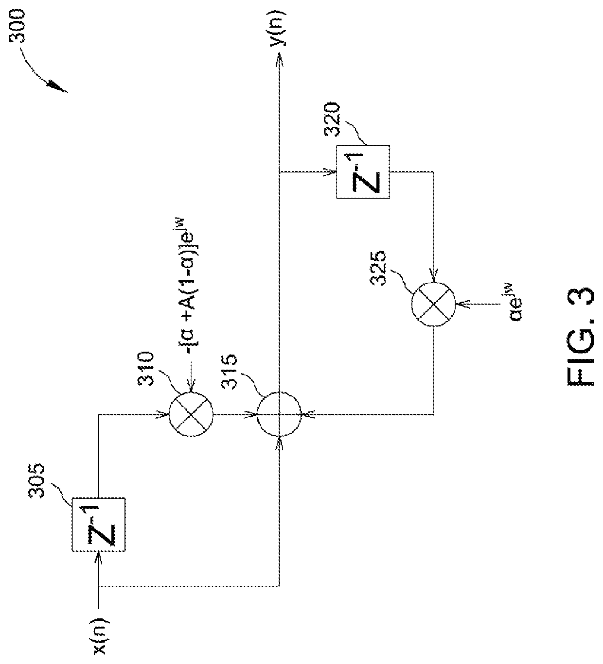
[0020]FIG. 3 shows a circuit diagram of a notch filter 300 according to the present invention. The notch filter 300 includes a delay circuit 305 (serving as a buffer), a multiplier 310, an adder 315, a delay circuit 320 (serving as a buffer) and a multiplier 325. The delay circuit 302 receives and delays an input signal x(n) to generate a delayed signal to the multiplier 310. According to a first parameter (i.e., −[α+A×(1−α)]×ejω, the multiplier 310 multiplies the first parameter by the delayed signal to generate an output signal to the adder 315. The adder 315, coupled to the multiplier 310, the delay circuit 320 and the multiplier 325, adds the input signal x(n), the output signal of the multiplier 310 and the output signal of the multiplier 325 to generate an output signal y(n). The delay circuit 320 receives and delays the output signal y(n) to generate a delayed signal to the multiplier 325. According to a second parameter (i.e., α×ejω), the multiplier 325 multiples the second ...
third embodiment
[0025]FIG. 4 shows a circuit diagram of a filter circuit 401 according to the present invention. The filter circuit 401 includes a notch filter 400 and an adaptive estimating circuit 405. The circuit structure of the notch filter 400 may be implemented by the notch filter 100 in FIG. 1 or the notch filter 300 in FIG. 3. The adaptive estimating circuit 405 includes a delay circuit 410 (including n delay circuits connected in series, with the first delay circuit receiving the input signal), a multiplication circuit 415 (including n multipliers), an addition circuit 420 (including n adders connected in series) and an adder 425, where n is a value greater than or equal to 2. Each multiplier is connected to an output of the corresponding delay circuit, and multiples the output of the corresponding multiplier by a corresponding parameter (C1, C2, . . . and Cn) to generate a corresponding product to a corresponding adder among the adders 420. The n adders add the products of the individual...
PUM
 Abstract
Description
Claims
Application Information


