Light engine based on silicon photonics TSV interposer

a silicon photonics and interposer technology, applied in the direction of instruments, optical elements, optical waveguide light guides, etc., can solve the problems of consuming a lot of pcb space and requiring internet and mobile applications to transfer photos, videos, music, etc., and achieves less pcb space and better rf performance.

Active Publication Date: 2020-02-18
MARVELL ASIA PTE LTD
View PDF10 Cites 18 Cited by
  • Summary
  • Abstract
  • Description
  • Claims
  • Application Information

AI Technical Summary

Benefits of technology

[0010]Many benefits are provided with the improvement according to the present invention. In certain embodiments, the present invention provides a replacement of wire bonds by “bump-TSV-trace-bump” or “bump-trace-TSV-trace-bump” in a chip scale package (CSP) with better RF performance. In some embodiments, the chip-scale-package using (through-silicon via) TSV silicon photonics interposer consumes less PCB space. In some other embodiments, with the TSV process, multilayer capacitors (MLCs) can be fabricated simultaneously to eliminate the use of stand-alone DC blocking capacitors and by-pass capacitors on PCB. The present invention achieves these benefits and others in the context of broadband communication technology. However, a further understanding of the nature and advantages of the present invention may be realized by reference to the latter portions of the specification and attached drawings.

Problems solved by technology

But Internet and mobile applications continuously demand a huge amount of bandwidth for transferring photo, video, music, and other multimedia files.

Method used


Image

  • Light engine based on silicon photonics TSV interposer
  • Light engine based on silicon photonics TSV interposer
  • Light engine based on silicon photonics TSV interposer

Examples


Embodiment Construction

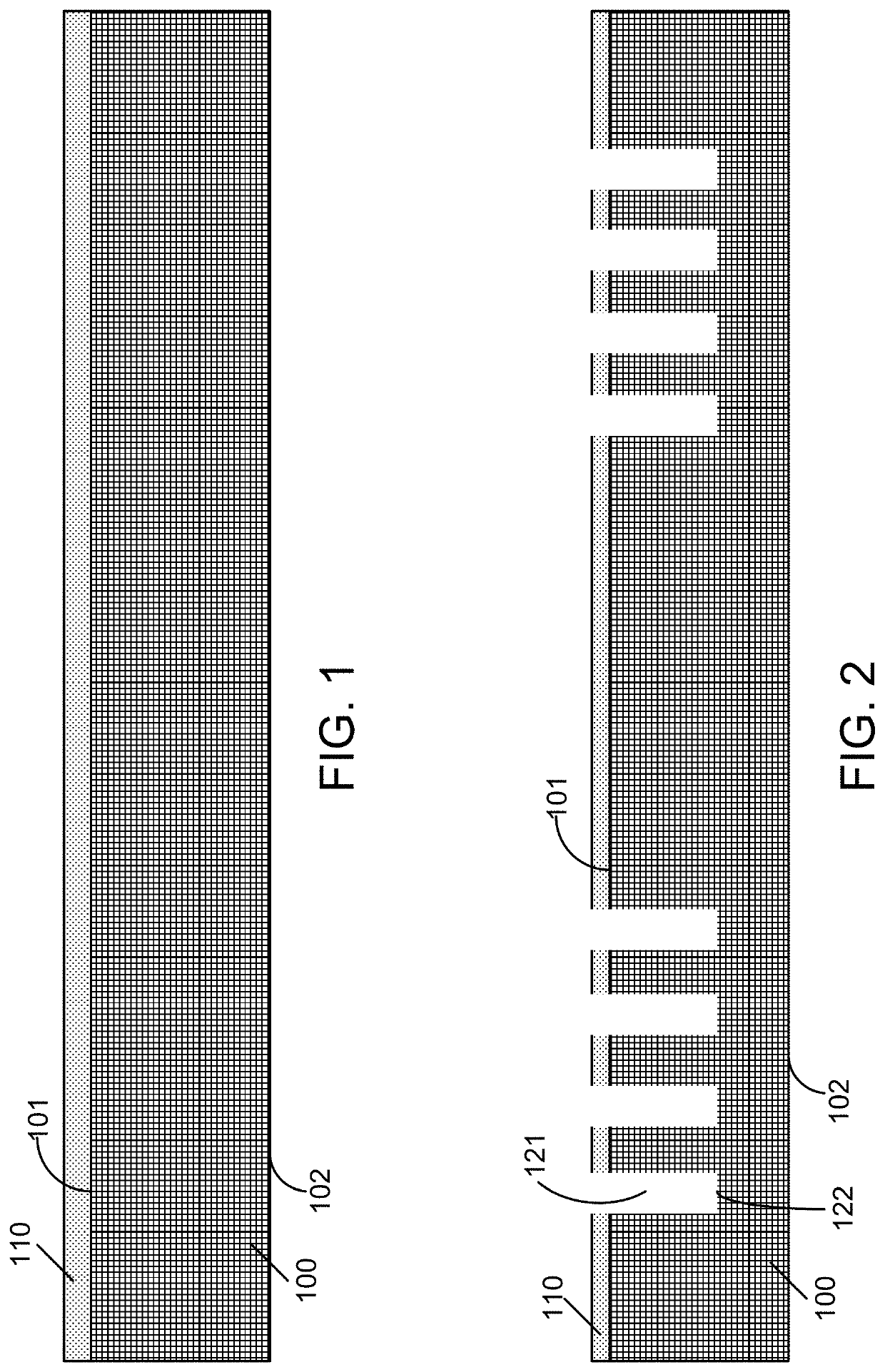
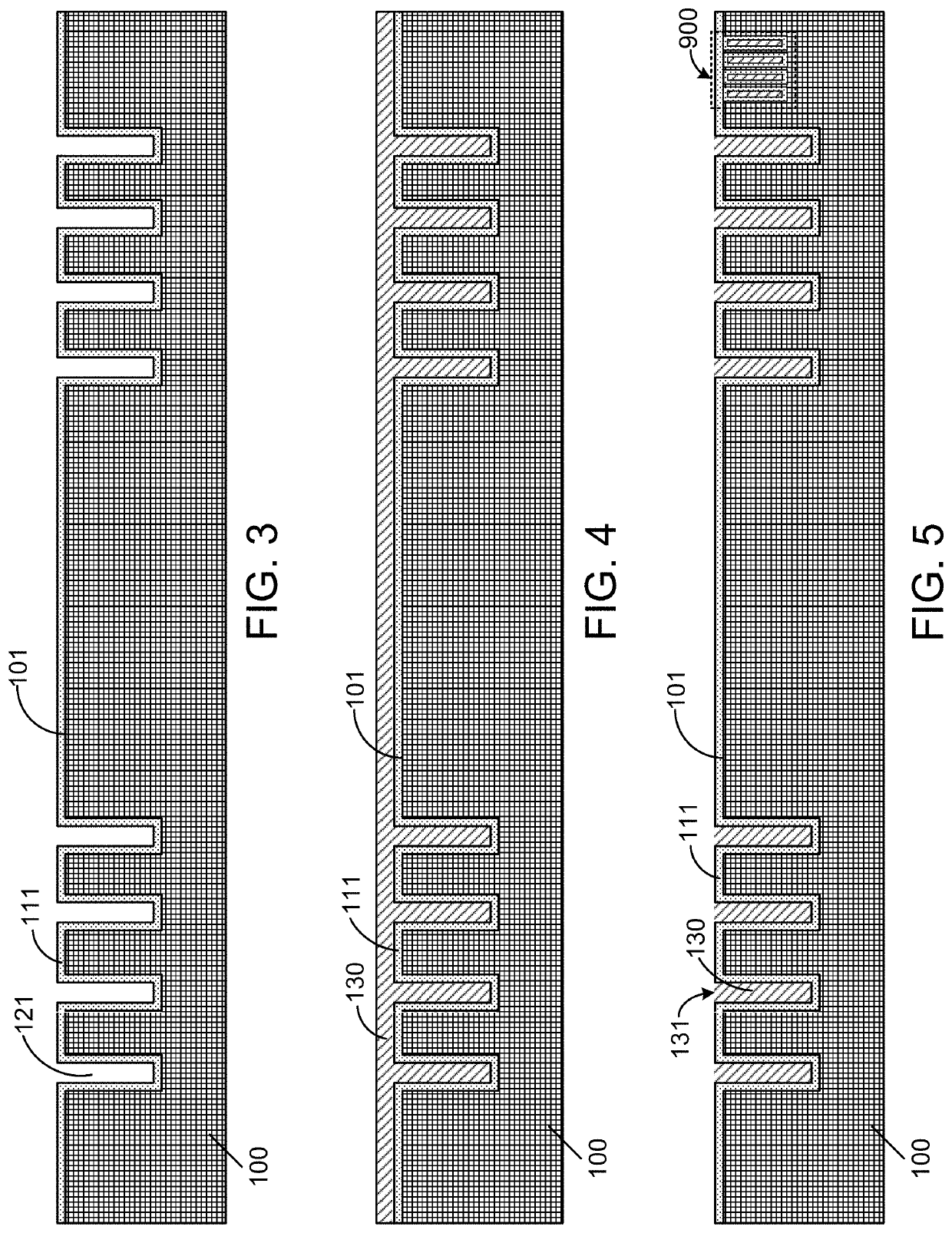
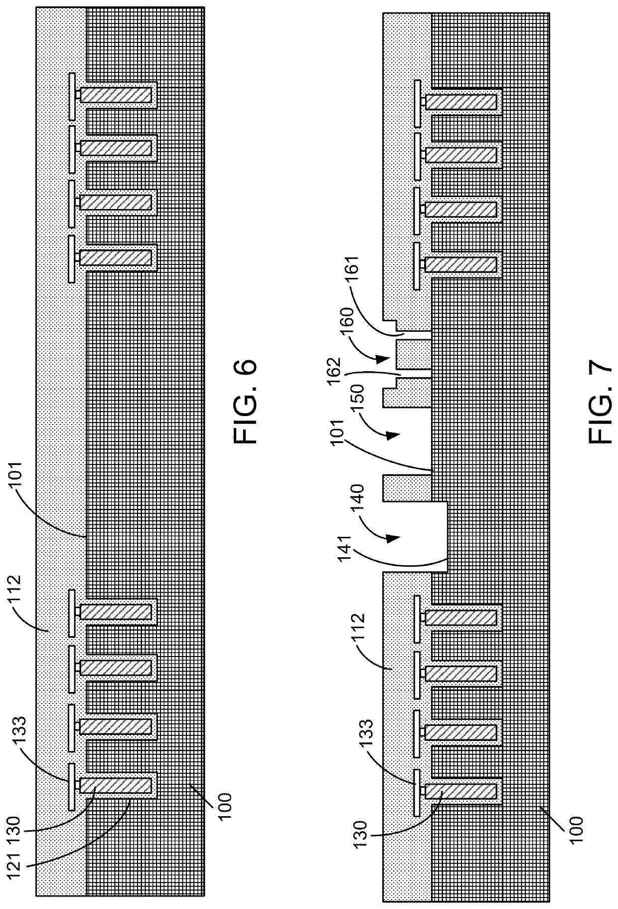
[0015]The present disclosure is related to manufacture technique for integrated silicon photonics device. More particularly, the invention provides a light engine based on a silicon photonics through-silicon via interposer and a method of making the same. In certain embodiments, the invention is applied for high data rate optical communication, though other applications are possible.

[0016]The following description is presented to enable one of ordinary skill in the art to make and use the invention and to incorporate it in the context of particular applications. Various modifications, as well as a variety of uses in different applications will be readily apparent to those skilled in the art, and the general principles defined herein may be applied to a wide range of embodiments. Thus, the present invention is not intended to be limited to the embodiments presented, but is to be accorded the widest scope consistent with the principles and novel features disclosed herein.

[0017]In the ...


PUM

PropertyMeasurementUnit
thicknessaaaaaaaaaa
depthaaaaaaaaaa
depthaaaaaaaaaa

Abstract

A method for forming a silicon photonics interposer having through-silicon vias (TSVs). The method includes forming vias in a front side of a silicon substrate and defining primary structures for forming optical devices in the front side. Additionally, the method includes bonding a first handle wafer to the front side and thinning down the silicon substrate from the back side and forming bumps at the back side to couple with a conductive material in the vias. Furthermore, the method includes bonding a second handle wafer to the back side and debonding the first handle wafer from the front side to form secondary structures based on the primary structures. Moreover, the method includes forming pads at the front side to couple with the bumps at the back side before completing final structures based on the secondary structures and debonding the second handle wafer from the back side.

Description

BACKGROUND OF THE INVENTION[0001]The present disclosure is related to manufacture technique for integrated silicon photonics device, and particularly to a light engine based on a silicon photonics through-silicon via interposer and a method of making the same.[0002]As science and technology are updated rapidly, processing speed and capacity of the computer increase correspondingly. The need for optical interconnect for high-performance computing and data center applications are indispensable with increasing demand. An optical communication system includes both electrical devices and optical devices, devices for converting electrical signal and optical signal back and forth, and devices for processing these signals. With the advances of optical communication technology and applications driven by the market demand on increasing bandwidth and decreasing package footprint, more intensive effort and progress have been seen in the development of electro-photonic integrated circuits on sil...

Claims


Application Information

Patent Timeline
Patent Type & Authority Patents(United States)
IPC IPC(8): H01L21/768G02B6/42H01L25/16H01L23/00H01L23/538G02B6/12
CPCH01L24/81H01L23/5384H01L25/167H01L24/17G02B6/428H01L2924/12042H01L2924/157H01L2924/14G02B2006/12061H01L21/768H01L21/76898G02B6/4243H01L2224/16238H01L2924/15311H01L2924/15159H01L21/6835H01L24/16H01L2221/68327H01L2221/6834
Inventor DING, LIANGNAGARAJAN, RADHAKRISHNAN L.
Owner MARVELL ASIA PTE LTD
Why Eureka
Try Eureka