Light-receiving element, manufacturing method of the same, imaging device, and electronic apparatus
a technology of light-emitting elements and manufacturing methods, applied in the direction of electrical apparatus, semiconductor devices, radio frequency controlled devices, etc., can solve problems such as signal crosstalk, and achieve the effect of suppressing signal crosstalk and easy doping of selective regions of photoelectric conversion layers
Active Publication Date: 2020-03-03
SONY CORP
View PDF26 Cites 0 Cited by
- Summary
- Abstract
- Description
- Claims
- Application Information
AI Technical Summary
Benefits of technology
Problems solved by technology
However, in an image sensor using such a compound semiconductor described above, a technology to separate a photoelectric conversion layer for each pixel has not been established, thus a photoelectric conversion layer is formed as a layer common to each pixel.
Accordingly, an electric charge generated on the photoelectric conversion layer moves to an adjacent pixel, which causes signal crosstalk.
Method used
View moreImage
Smart ImageViewing Examples
Examples
first embodiment (
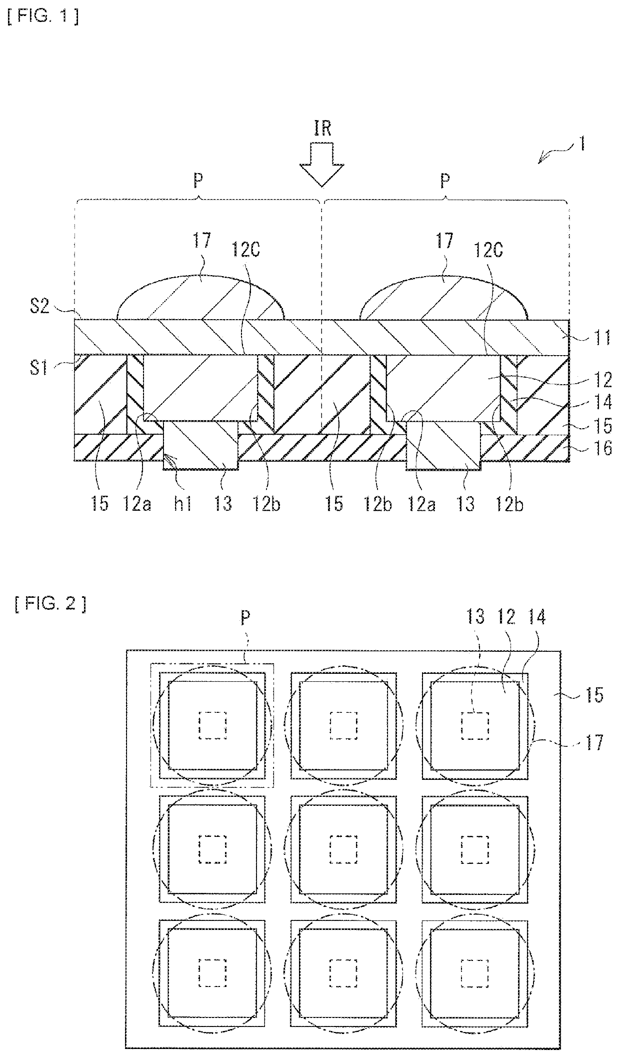
1. First Embodiment (An example of a light-receiving element provided with an insulating film that surrounds each of a plurality of photoelectric conversion layers)
second embodiment (
2. Second Embodiment (An example of a light-receiving element in a case where each photoelectric conversion layer is formed by using a Si substrate)
modification example 1 (
3. Modification Example 1 (An example of a case where two electrodes are provided)
Login to View More PUM
| Property | Measurement | Unit |
|---|---|---|
| band gap | aaaaa | aaaaa |
| band gap | aaaaa | aaaaa |
| speed | aaaaa | aaaaa |
Abstract
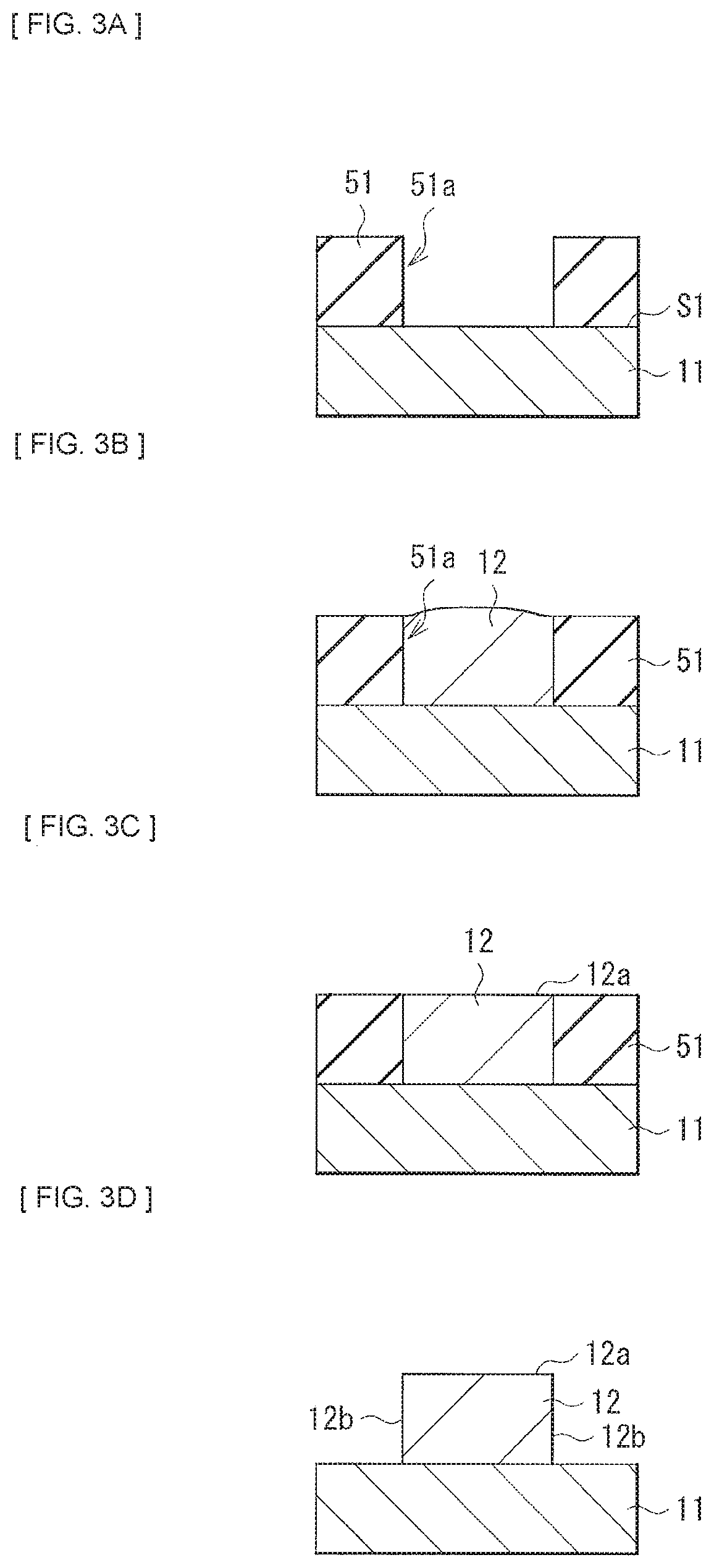
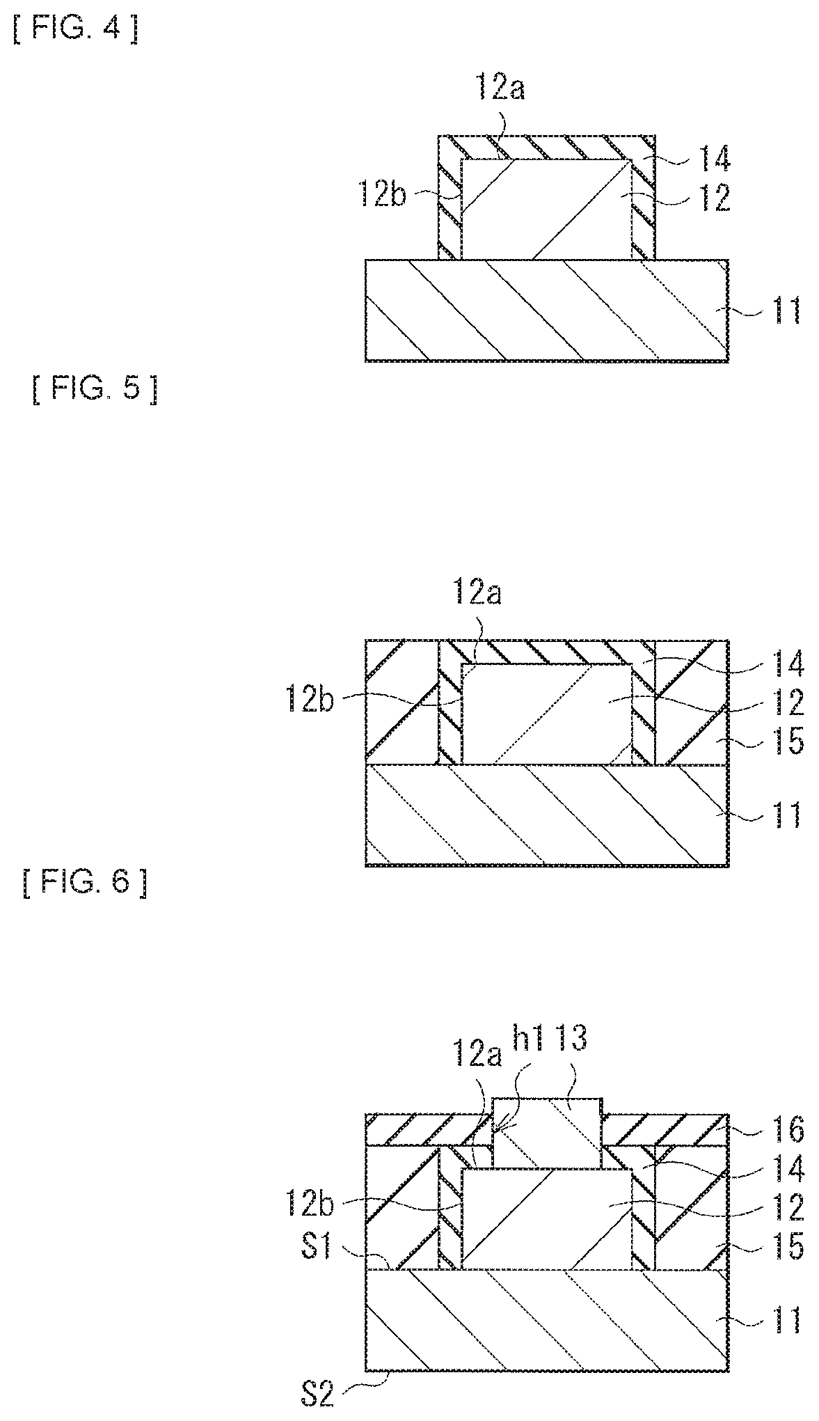
This light-receiving element includes a plurality of photoelectric conversion layers, each of which includes a compound semiconductor, and absorbs a wavelength in an infrared region to generate an electric charge, and an insulating film that is provided to surround each of the plurality of photoelectric conversion layers.
Description
CROSS REFERENCE TO RELATED APPLICATIONS[0001]This application is a U.S. National Phase of International Patent Application No. PCT / JP2016 / 088923 filed on Dec. 27, 2016, which claims priority benefit of Japanese Patent Application No. JP 2016-004158 filed in the Japan Patent Office on Jan. 13, 2016 and also claims priority benefit of Japanese Patent Application No. JP 2016-220779 filed in the Japan Patent Office on Nov. 11, 2016. Each of the above-referenced applications is hereby incorporated herein by reference in its entirety.TECHNICAL FIELD[0002]The disclosure relates to a light-receiving element used in, for example, an infrared sensor or the like and its manufacturing method, an imaging device, and an electronic apparatus.BACKGROUND ART[0003]An image sensor (an infrared sensor) having sensitivity in an infrared region has been commercialized recently. In a light-receiving element used in this infrared sensor, a photoelectric conversion layer including a group III-V semiconducto...
Claims
Login to View More Application Information
Patent Timeline
 Patent Type & Authority Patents(United States)
IPC IPC(8): H01L27/146H01L31/0224H01L31/0304H01L31/18
CPCH01L31/0224H01L27/14649H01L31/1868H01L31/1844H01L31/03046H01L27/14627H01L27/14694H01L27/1446Y02E10/544
Inventor YOSHIDA, SHINICHI
Owner SONY CORP


