Micro LED structure and method of manufacturing same
a micro-lead and led technology, applied in the direction of semiconductor devices, semiconductor/solid-state device details, electrical apparatus, etc., can solve the problems of affecting the electrical connection of each micro-lead and the addition of equipmen
- Summary
- Abstract
- Description
- Claims
- Application Information
AI Technical Summary
Benefits of technology
Problems solved by technology
Method used
Image

Examples
first embodiment
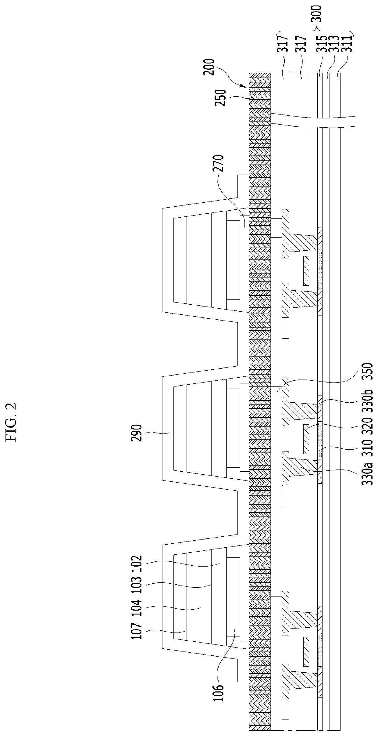
[0050]FIG. 2 is a view illustrating a micro LED structure according to a first embodiment of the present invention.
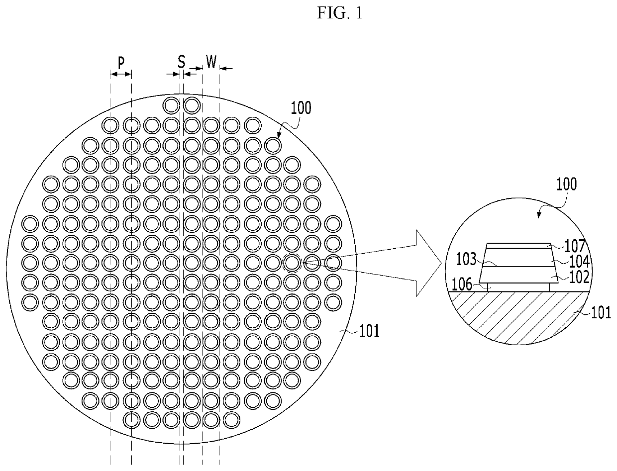
[0051]Hereinafter, a circuit board 300 on which the micro LEDs 100 illustrated in FIG. 1 are mounted will be described.
[0052]The circuit board 300 driving the micro LEDs 100 includes various materials. For example, the circuit board 300 may be made of a transparent glass material having SiO2 as a main component. However, components of the circuit board 300 are not limited to this, and the circuit board 300 may be made of a transparent plastic material and thus have solubility. The plastic material may be an insulating organic substance selected from the group consisting of polyethersulfone (PES), polyacrylates (PARs), polyetherimide (PEI), polyethylene napthalate (PEN), polyethylene terephthalate (PET), polyphenylene sulfide (PPS), polyarylate, polyimide, polycarbonate (PC), cellulose triacetate (TAC), and cellulose acetate propionate (CAP).
[0053]In the case of a bottom...
second embodiment
[0085]Hereinafter, a second embodiment of the present invention will be described. It should be noted that the embodiment described below will be described with particular emphasis on characteristic components as compared with the first embodiment, and descriptions of the same or similar components as those of the first embodiment will be omitted.
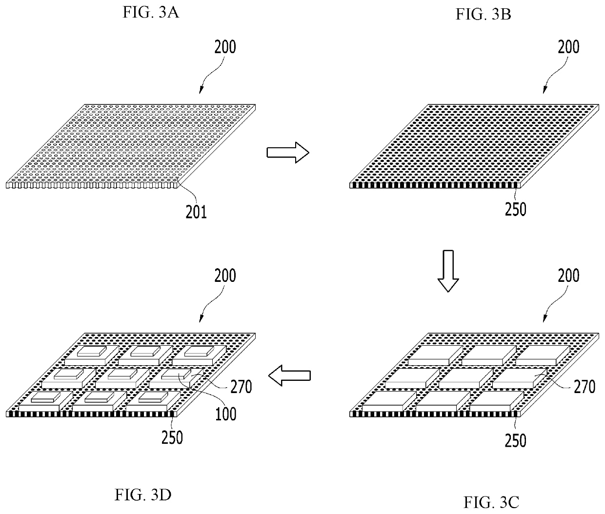
[0086]FIG. 4 is a cross-sectional view illustrating a micro LED structure according to the second embodiment of the present invention. The micro LED structure according to the second embodiment of the present invention is different from the first embodiment in a region where the conductive material 250 is filled. In the first embodiment, the entire pores 201 of the anodic oxide film 200 are filled with the conductive material 250. However, in the second embodiment, the conductive material 250 is filled only in the pores 201 of a region corresponding to the region where the metal pad 270 is provided. Here, the region corresponding to the reg...
third embodiment
[0094]Hereinafter, a third embodiment of the present invention will be described. It should be noted that the embodiment described below will be described with particular emphasis on characteristic components as compared with the first embodiment, and descriptions of the same or similar components as those of the first embodiment will be omitted.
[0095]FIG. 6 is a cross-sectional view illustrating a micro LED structure according to the third embodiment of the present invention. The micro LED structure according to the third embodiment of the present invention differs from the first embodiment in a region where the conductive material 250 is filled. In the first embodiment, the entire pores 201 of the anodic oxide film 200 are filled with the conductive material 250. However, the third embodiment provides a through-hole 203 having an opening area larger than that of an individual pore 201, and the conductive material 250 is filled in the through-hole 203. In other words, the through-h...
PUM
| Property | Measurement | Unit |
|---|---|---|
| size | aaaaa | aaaaa |
| size | aaaaa | aaaaa |
| anisotropic conductive anodic | aaaaa | aaaaa |
Abstract
Description
Claims
Application Information
 - R&D
- Intellectual Property
- Life Sciences
- Materials
- Tech Scout
- Unparalleled Data Quality
- Higher Quality Content
- 60% Fewer Hallucinations
Browse by: Latest US Patents, China's latest patents, Technical Efficacy Thesaurus, Application Domain, Technology Topic, Popular Technical Reports.
© 2025 PatSnap. All rights reserved.Legal|Privacy policy|Modern Slavery Act Transparency Statement|Sitemap|About US| Contact US: help@patsnap.com